Although the actual diagram of the Nvidia GK104 GPU has been seen earlier, now we get a full explanation regarding GK104 CUDA core impressive 1536 number as well as more details regarding the actual structure of the GK104.
As rumoured earlier, Nvidia's GK104 is based on 28nm manufacturing process, has a die size of 294mm2 and features 3.54 billion transistors. The 1536 CUDA core number has been quite interesting and it is basically three time more than what we had a chance to see on the Fermi based GTX 680.
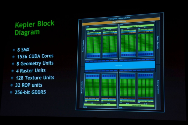
According to leaked info at HKEPC site and pictures from what appears to be Nvidia's presentation, the GK104 GPU starts with the GigaThread Engine placed between the GPU and the PCI-Express 3.0 interface. The GPU consists of four graphics processing clusters, or shortly GPCs, which share the same L2 cache and feature single raster engine each and two streaming multiprocessors or SMs that are now called SMX.
Each SMX features a PolyMorph Engine 2.0, Instruction, Texture, shared L1 and other caches, 192 CUDA cores accompanied by load/store (LD/ST) and special function units. If you add every GPC up, you'll get a total of four Raster Units, eight Geometry Units, 32 ROPs and 128 Texture Units. Since every of those four GPCs has two SMXs, every SMX has 192 CUDA Cores, it is quite easy to get to that magic 1536 CUDA Core number.
The GK104 is quite similar to the GF104 Fermi GPU but with a larger number of CUDA cores per SM, or in this case SMX. While GF104 had two GPC with four SMs each, GK104 has four GPCs with two SMs each. It also has more texture units per SM, upgraded Polymorph Engine, two more rasters, same amount of ROPs and geometry units, and a same 4x64-bit memory controller that adds to 256-bit wide memory interface, but the idea is pretty much the same.
Of course, we are looking forward to see some official reviews. You can check out the original GK104 GPU diagram screenshots here.