Index
- Nvidia officially launches GTX 670
- 3DMark11
- Crysis 2
- Aliens vs Predator
- Metro 2033
- Tessellation: Heaven
- Performance conclusion
- EVGA GeForce GTX 670 Superclocked
- Gainward GeForce GTX 670 Phantom
- Gainward GeForce GTX 670 2GB
- ASUS GeForce GTX 670 DirectCU II TOP (OC Edition)
- Galaxy GeForce GTX 670 GC
- Galaxy GeForce GTX 670 2GB
- Gigabyte GeForce GTX 670 GV-N670OC-2GD
- MSI N670GTX-PM2D2GD5/OC
- Zotac GeForce GTX 670 AMP! Edition
- All Pages
Review: Bunch of non reference designs, impresive performance
Nvidia launched its GTX 670 card today and it’s only the third card based on Kepler architecture. GTX 670 brings all the key features of the GTX 680, but in a more affordable package. Launching the GTX 670 went pretty well since all Nvidia’s partners received a green light for overclocking and custom designs. We got EVGA GTX 670 SuperClocked and Gainward GTX 670 Phantom graphics cards, both of which come with high factory overclocks. Nvidia gave the rest of its partners enough time to make a card to their liking. We’ve seen much creativity in this respect, starting with a single slot GTX 670, different two and even three-fan coolers, etc. So, let’s move onto the GTX 670.
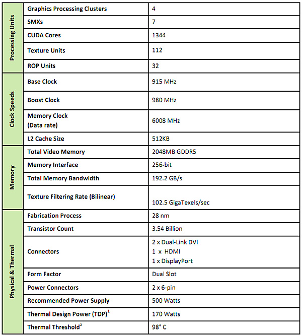
GTX 680 boasts an efficient GPU and since the GTX 670 was made in the same mould, i.e. uses the GK104 GPU, you can expect a nice performance per watt ratio. Compared to the GTX 470, users are looking at 2.5x better performance per watt ratio. Compared to the GTX 570, this ratio is more than 2 times better.
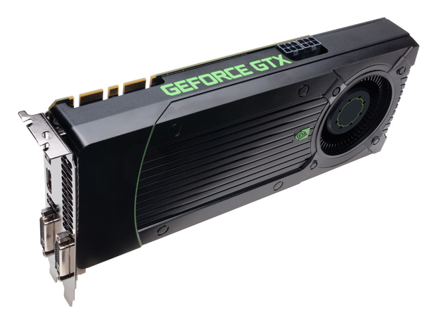
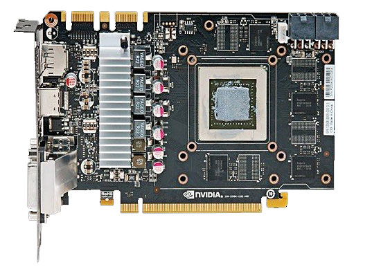
You’ve probably noticed that the power connectors are close to the center of the card, but there’s a good reason for that. Namely, the PCB ends there, whereas the rest is the cooler. The following photo shows our GTX 670 from the rear. GTX 670 cards come with two 6-pin power connectors. Typical board power is about 141W while the TDP is at 170W.
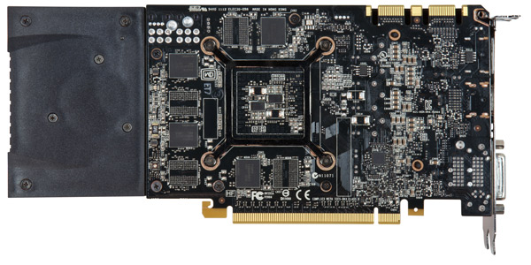
Interestingly enough, the memory modules were spread out in a way where each chip faces the opposite side of its predecessor/successor. The card packs eight memory chips totaling at 2GB of GDDR5 memory. Good news for Nvidia fans is that the company kept the identical memory system used on its GTX 680 card, meaning four 64-bit memory controllers (256-bit memory interface) and 2GB of GDDR5 memory. The memory runs at 1502MHz (6008MHz effectively), again just like the GTX 680.
GTX 680 comes with eight SMX units and 1536 CUDA cores, whereas the GTX 670 comes with seven SMX units and 1344 CUDA cores. Base clock for the GPU is 915MHz while the typical value for Boost Clock is 980MHz. We’ve seen that some partners were quite bold and set the base clock beyond 1GHz at launch. However, it’s not a miracle that the GK104 would run beyond 1GHz, since the GTX 680’s base clock is 1006MHz.
The GTX 670 comes with two SLI connectors usually found on Nvidia’s high end cards. This means that users can stack more cards in a Quad GTX 670 system. The reference GTX 670 card is 9.5“ or 24.1cm.
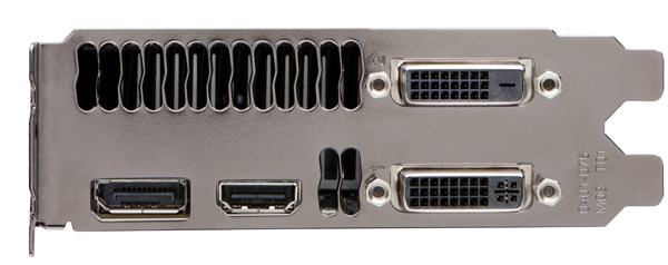
Video outs include two dual-link DVIs (only one is VGA capable) and standard HDMI and DisplayPort connectors. Note that all four outs can be used simultaneously.
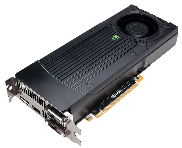
Although the GTX 670 is 24.1cm long, the PCB is only 17.2cm. Nvidia moved the power circuitry from its usual spot at the end of the card. This left empty space at the end of the PCB, so the company simply cut it off and saved on materials.
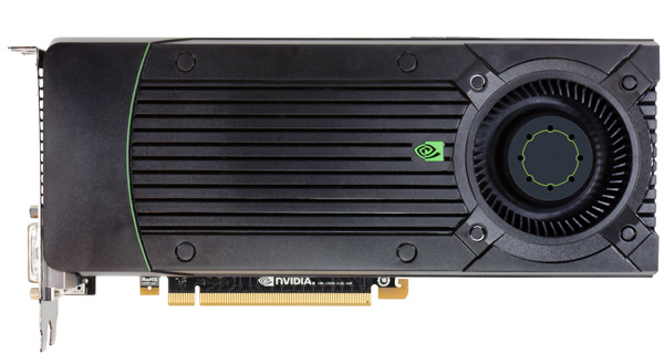
Since the GPU is much like the one used on GTX 680 cards, Nvidia had to ensure adequate cooling. This is why the company used a quite hefty dual slot cooler, which is actually only a centimeter shorter than the one on GTX 680. GTX 680 and 670’s fans are the same type and size.
Suggested pricing stands at 329 EURO EX VAT / $399 USD.