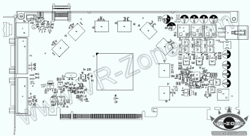
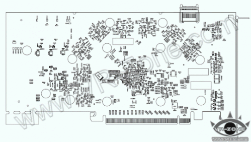
Earlier this week, we mentioned that Nvidia's 55nm Geforce GTS 240 is basically a rebranded, overclocked edition of the popular 55nm 9800GT based on G92 architecture. Not only will the card have a new PCB layout, but it will also feature power design changes in the VRM area.
The new P361 printed circuit board for the card is internally codenamed D10P2 as opposed to the board on the 9800GT codenamed G92GT. The P361 PCB will house the G92b core and eight GDDR3 memory chips connected to the GPU across a 256-bit wide bus.
However, the new hardware changes of the GTS 240 lie within the Voltage regulation module area of the PCB, mainly the adoption of a 3 + 1 phase design. The PCB draws power from a 6-pin PCI-Express power connector as before, and there is a single SLI bridge connector for 2-way SLI.
As far as cooling is concerned, we expect most partners to adopt a single-slot design, as the 55nm G92b core runs noticeably cooler than its 65nm G92 counterpart.
Pictures courtesy of VR-Zone


Published in
Graphics
55nm Geforce GTS 240 launches in April

New PCB codenamed D10P2
