Since we are just a few days from the official launch date set for February 18th, we now have some of the first pictures of Nvidia's GTX 750 taken apart by the ChinaDIY team and pictured in full detail.
As we wrote earlier, Nvidia's Maxwell architecture will bring some impressive power efficiency improvements, despite the fact that the first batch of the graphics card based on the Maxwell architecture will be actually based on current 28nm manufacturing process. While the GM107 and the GM108 will stay at 28nm, Nvidia is waiting for TSMC's 20nm node process to release its higher-end GPUs based on Maxwell architecture, so we are quite sure there will be some even more impressive performance per Watt numbers once those come.
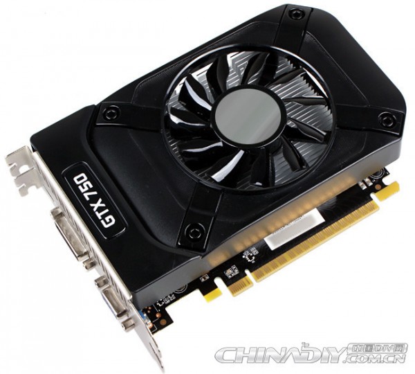
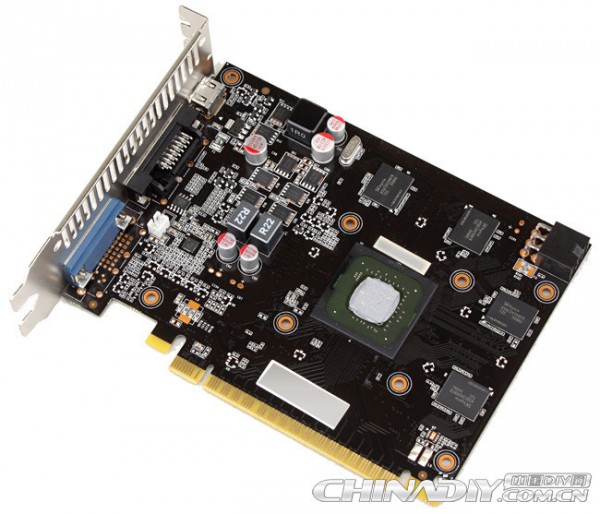
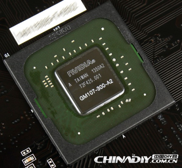
Although we have no idea from which partner this GTX 750 comes, it features a rather simple dual-slot cooler and standard PCB design with a 2+1-phase VRM which draws power from a single 6-pin PCI-Express power connector. The GM107-300-A2 GPU has been also pictured in full details and since it will have a rather low TDP, there is no need for hefty custom coolers as this is still a mainstream graphics card.
As we reported earlier, both the GTX 750 and the GTX 750 Ti are expected to show up later this month. You can check out the rest of the pictures over at ChinaDIY.com.cn.