
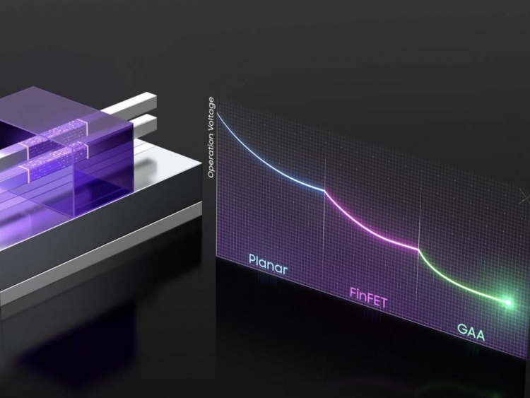
It has been known that Samsung is working on Gate-All-Around FET technology that will bring much better control of the transistor channel, less leakage smaller nodes. But now Samsung has detailed its Multi Bridge Channel FET technology for 3nm manufacturing process, [MBCFET].
According to the German techsite Hardwareluxx, MCBFET is a part of GAAFETs, meaning that the GAAFET is not one product, but rather a class of different ones. Samsung says that the technology will use 50 percent less power while delivering 30 per cent more performance. There is going to be a big density gain as well, where Samsung predicts there will be around 45 percent less silicon space taken per one transistor.
The comparisons are against an unspecified 7 nm process, but this is likely to be Samsung's own which uses FinFETs. The technology allows the stacking of transistors on top of each other, which makes it use inherently less space compared to bog standard FinFET.
MCBFET GAA transistors make its transistor width flexible, it means that the overall stacked transistor can be as wide as the designer likes and adjusted for low-power or high-performance.
All major semiconductor manufacturers are working on GAA transistors. At Samsung these are now called MBCFET, Intel does not yet have a name for its next generation of 3D transistors.