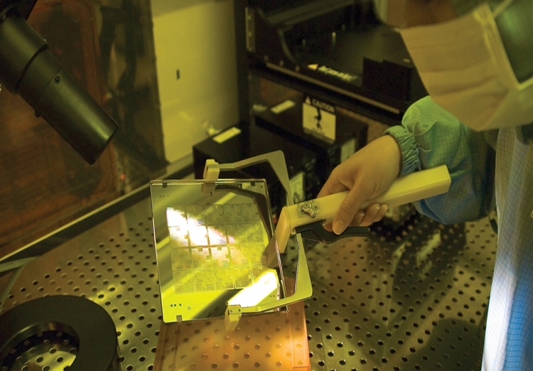
According to the Electronic Times, Samsung said that it will soon be completing development of Low-Power Compact (LPC) 14-nano FinFET process. Strategic partners of Samsung’s foundry business are predicting that this process will be used in anger by the end of the year.
All this is moving fast Samsung mass-produced Low Power Early (LPE) Chips, which are 1st generation chips just last year. It has just mass-produced second 2nd generation 14-nano LPP66 (Low Power Plus) chips that have 15 per cent lesser electricity consumption compared to LPE chips.
The Exynos 8 Octa Series and Qualcomm’s Snapdragon 443 820 which is under the bonnet of the Galaxy S7 are mass-produced through 14-nano LPP process.
Samsung’s third generation process reduces the number of masks that are used for wafer manufacturing process. It is expected that 14 nano will be around for as long as 28 nano was.
Even when 10-nano and 7-nano processes are developed, there will be many fabless manufacturing companies will still use cost-efficient 14-nano process.
Qualcomm, Samsung and Mediatek recently introduced new 14 and 16-nano AP products that are inexpensive. They will be used for Snapdragon 443 625, Exynos 7870, and Helio P20, and this indicates that a number of chips produced by 14-nano process will increase.
Samsung’s 14-nano LPC process, will start a war with Taiwan’s TSMC in a battle to secure customers. TSMC has three types of 16-nano FinFET processes. It’s first 16-nano FinFET process arrived at the end of 2014.
.