
On Monday, Taiwan Semiconductor Manufacturing Company (TSMC) held a groundbreaking ceremony at the South Taiwan Science Park in Tainan, Taiwan to celebrate the beginning of Phase 5 construction at its Fab 14. In a nutshell, Fab 14 is TSMC's second 12-inch (300mm) wafer facility alongside Fab 12, and Phase 1 of this facility began volume production eight years ago in 2004.
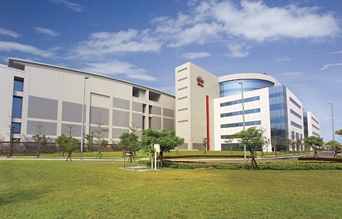
TSMC's Fab 14 facility in Tainan, Taiwan
Nevertheless, Fab 14 has a current capacity of 550,000 12-inch wafers per quarter, making it the world's largest 12-inch fab. TSMC's new Phase 5 expansion at Fab 14 will be the company's second 20nm-capable fab following its current 20nm capacity at Fab 12 Phase 6 in Hsinchu. According to the company's plans, Fab 12 Phase 6 in Hsinchu will begin 20nm volume production sometime in 2013, while the new Fab 14 Phase 5 expansion in Tainan will begin 20nm volume production in Q1 2014.
Combined with its Fab 12 Phase 6, TSMC's total cleanroom area for 20nm production will soon reach 87,000 square meters – equal to more than 11 soccer fields and four times larger than a typical 12-inch fab – and will further strengthen TSMC's global competitiveness in advanced technologies.
As an incentive, the new Phase 5 expansion at Fab 14 will also create another 4,500 high-quality job opportunities for the Taiwanese economy, adding to its current 4,600 employee staff and injecting fresh momentum into TSMC's expanding competitive reach.


