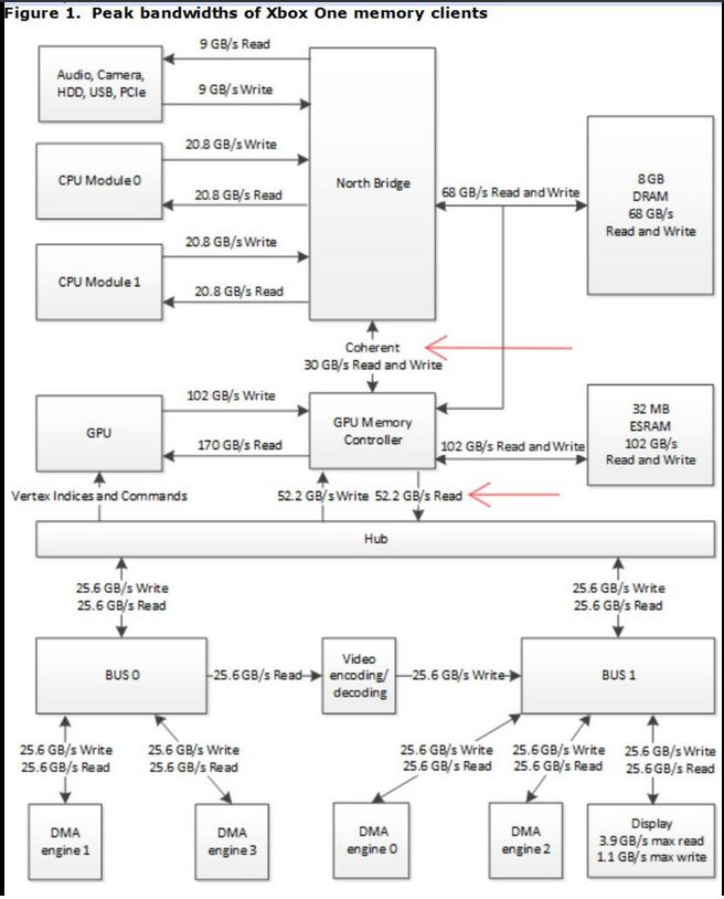
The slides in the Tweet come from a paper about CPUs, APUs and GPUs published last month with AMD Corporate Fellow and graphics engineer, Mike Mantor listed as a contributor.
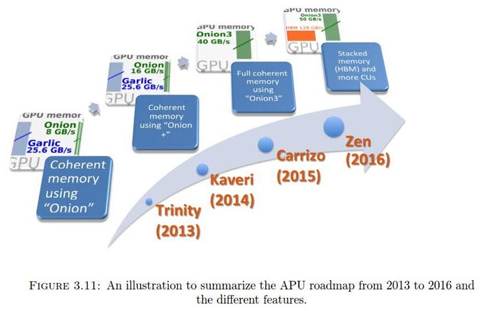
An AMD APU roadmap summary slide shows progression of this processor from Trinity, to Kaveri, to the current generation Carrizo, to Zen-based APUs.
The APU total memory bandwidth has risen from 8GB/s back in 2013 to 50GB/s later this year when the Zen APU gets released. The Zen APU will be built with 128GB/s stacked memory (HBM) and "more CUs", which we assume to be additional graphic compute units.
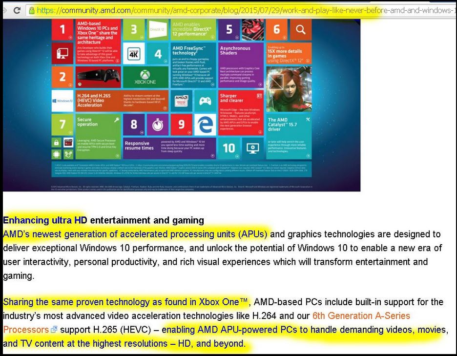
It looks like the Zen APU will be marketed as 'enhancing ultra HD entertainment and gaming' and PCs with the new Zen APU will push further AMD's plan to make a single chip to provide robust, rich visual experiences to Windows 10 PC builds. This all fits into what we have been told already. There were some hints last year about AMD's doings which pointed in this direction and time scale.
Cue comments below how Nvidia might as well surrender now along with others saying that Nvidia will clean Zen’s clock before the thread degenerates into abuse about a fanboy’s mother.


