It looks like we might never see 20nm GPUs from either Nvidia or AMD. From what we know, both companies spent a lot of time looking into the new 20nm manufacturing process and they have decided that it is simply not viable for GPUs.
Yields are not where they are supposed to be and from a business perspective it doesn’t make sense to design and produce chips that would end up with very low yields. At this point we do not expect to see any high-end chips in 20nm, as there are obvious manufacturing obstacles and both companies might even skip the 20nm process altogether and move directly to 16nm FinFET.
16nm FinFET GPUs coming in 2016
We expect 16nm FinFET based GPUs sometime 2016 and this manufacturing process will bring some rather innovative products worthy of an upgrade.
One might ask why Apple doesn’t appear to have problems with its 20nm A8 and A8X chips and we might have a partial answer for you. The Apple A8 chip has to stay under 2.5W TDP, the A8X used in the iPad Air 2 A8X has a maximum TDP of 4.5W.
GPUs such as Maxwell- and Hawaii-based parts used in the Geforce GTX 980 and Radeon R9 290X have TDPs in the 150-250W range and the size of the modern GPU is an order of magnitude bigger than the size of an iPhone SoC.
Die size conundrum
The Apple A8 has a die size of 89mm2 and while we can only assume that the more powerful A8X measures over 100 mm2. Nvidia’s 28nm Maxwell GM204 die measures 398 mm2, which is about four and a half times bigger in terms of sheer die size.
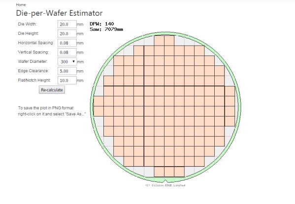
To put things in perspective, in a single 20nm 300mm wafer you can place more than 700 A8 dies, while Nvidia can get about 140 Maxwell 204 chips from a 28nm High K 300 mm wafer and in 20nm manufacturing it would be able to get more, as the individual die would be significantly smaller.
However, these 150-250W chips are completely different than low-power SoCs with TDPs of less than 5W. They are worlds apart and one can assume that with the high performance and clock of discrete GPUs, coupled with their sheer size, result in higher leakage and other issues. Making a chip 4.5 times bigger means that there is much more room for potential issues, leakage and yield problems.
Don’t despair, 28nm still has some life in it
Not all is lost. We all saw that Nvidia pulled off a small miracle with the 28nm Maxwell GM204 chip, as this 5.2 billion transistor chip has a TDP of just 165W.
Its predecessor, the Geforce GTX 780 based on the GK110 chip, ended up with a 250W TDP with 7.08 billion transistors and a massive 561mm2 die size. Maxwell is also faster than Kepler, at least in this iteration, yet they are both 28nm products.
We expect that AMD’s upcoming Fiji GPU to be substantially more efficient than the Hawaii XT chip used in last year’s Radeon R9 290X. However, the new part is coming in 2015.