Dyed green and looking rather similar to a mould pattern we have in our loo, the 610mm2 chip is magnified so that the various key functional component parts can be easily seen. The picture shows the chip's 15.3 billion transistors in all their glory and you can see how Nvidia has grouped everything together.
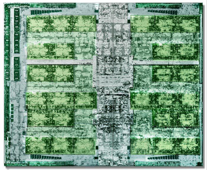
The darker green squares are the 30 Texture Processor Clusters. They consist of two (Streaming Multiprocessors for a total of 60. There are four NVLink interfaces can be seen on the left side and four HBM2 interfaces in pairs on the top and bottom. The middle is the thread scheduler and a few other bits we can't work out.
The HBM and NVLink are the important things as this will be the first Nvidia chip to use them. The fact that the HMB2 interfaces take up so little space is also important. .
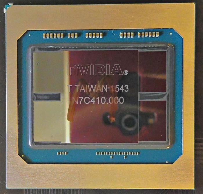
Nvidia also showed off a production GP100 package which was showed how closely the the GPU and HBM2 stacks are packaged. The four (16 GB) HMB2 memory stacks make up two thirds the of the GPU.