Index


Review: Faster, cooler, great performer
Nvidia launched its first Kepler based card GTX 680 on 22 of March. The goal was pretty much clear – retake some of the ground they lost to AMD. AMD has proudly sat on the single-GPU throne since the 22 of December, when it launched HD 7970 card. It took a lot of effort for Nvidia to achieve this goal, including redesigning the existing architecture to improve performance as well as consumption. The company did a good job and we’ll use Gainward’s GTX 680 as proof. Note that Gainward’s card is only a sticker away from the reference design.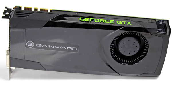
Gainward GTX 680 2GB runs at reference clocks, i.e. 1006MHz GPU and 6008MHz (GDDR5) memory. There are no shader clocks. The difference between Fermi and Kepler architecture lies in the fact that Nvidia equipped Kepler with more shader units. However, these shaders are now slower and run at GPU clocks. So, instead of doubling shader clocks, Kepler comes with double the amount of shaders. Nvidia made sure to boost the GTX 680’s performance and with that in mind, the company not only doubled the GTX 580’s shader count, but tripled it. This means that our today’s card boasts 1536 shader units (or CUDA cores), compared to the 512 units on GTX 580 cards. GK104 was made by TSMC in 28nm and packs 3.54 billion transistors. Note that while this is impressive enough, it’s still not enough to beat the HD 7970’s 4.31 billion. GTX 680 cards come with DX 11.1 and PCI-Express 3.0 support.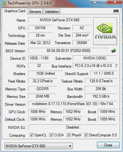
One of the things we paid a lot of attention to is the new self-tuning logic, i.e. GPU Boost. This tech fine-tunes clocks on the fly in order to squeeze out maximum juice from the GK104 GPU. The tech runs similarly to Intel’s Turbo Boost. Namely, when the GPU isn’t overloaded and has not exceeded the TDP, GPU Boost will auto-overclock.
Apart from juicing up the performance, Nvidia did a lot of work on power efficiency. You may recall that this was one of the bigger downsides of Nvidia’s last two generations (GTX 500/400), especially when compared to AMD’s offer.
Gainward’s box may be a bit too large for our taste but size tends to win over many customers. We saw some new pictures on the box and the name is now printed on the side of the box. This is probably a wise move as well, since it can be a bit problematic when the boxes are stacked. The package holds a driver CD, DVI-to-VGA converter and Molex-to-6-pin converter.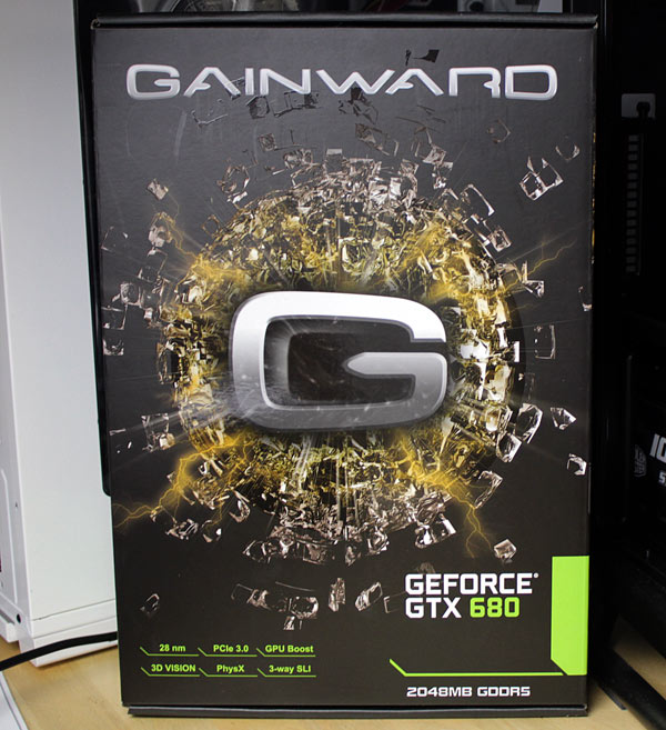
Geforce GTX 680 looks very much like its predecessor, GTX 580. However, a more detailed inspection reveals several important differences.
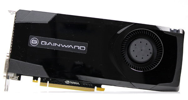
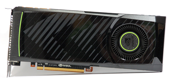
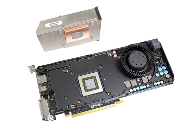
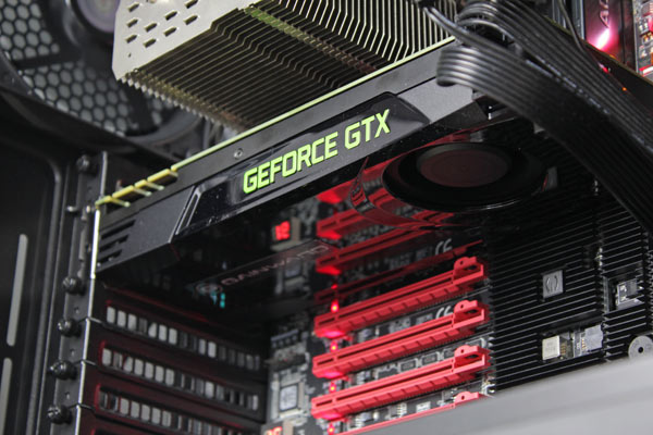
Looking at the front, we see that the cooler is blower-style and that the fan was placed towards the top of the card rather than dead center. Once we removed the cooler, we saw that the voltage regulation circuitry was placed horizontally in the lower part of the card, rather than vertically like on GTX 580 cards. It could be that the part of the cooler towards the GPU doesn’t get as hot this way. The cooler was designed to cool the GPU, memory and voltage regulation circuitry at the same time.
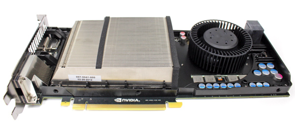
The GTX 680 is powered via two 6-pin power connectors. It’s interesting to see that Nvidia opted on stacked power connectors. We personally don’t like this as it makes the task of connecting cables much harder. When disconnecting the cables, you’ll have to take out the bottom one first and then the top one, which was rotated by 180 degrees. 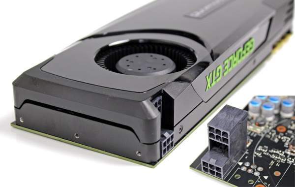
We already said that Nvidia implemented a type of auto-overclocking (GPU Boost), which monitors consumption and TDP and then changes clocks on the fly in order to maximize performance. Monitoring consumption come courtesy of the three INA219 power monitor chips (two for 6-pin power connectors and one for PCI-Express consumption).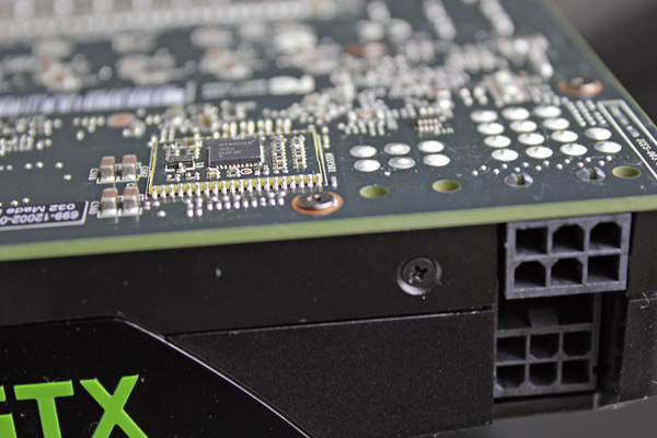
The memory is faster than ever before, which means Nvidia solved some important issues in this respect. The GTX 680 comes with 2GB GDDR5 memory that runs at 1502MHz (6008 MHZ GDDR5 effectively). The chips on Gainward’s card are made by Hynix, and carry the model number H5GQ2H24MFR-R0C. They are specified to run at 1500 MHz (6000 MHz GDDR5 effective).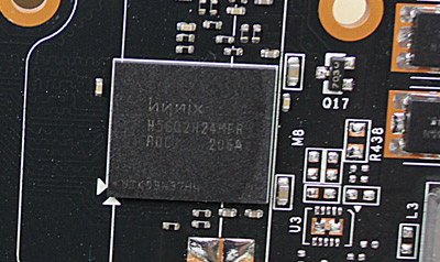
The card has a dual-link DVI port (with analog VGA), one dual-link DVI port (digital only), one standard HDMI and DisplayPort. Thanks to Nvidia’s new display output logic, Kepler based cards can support up to four displays.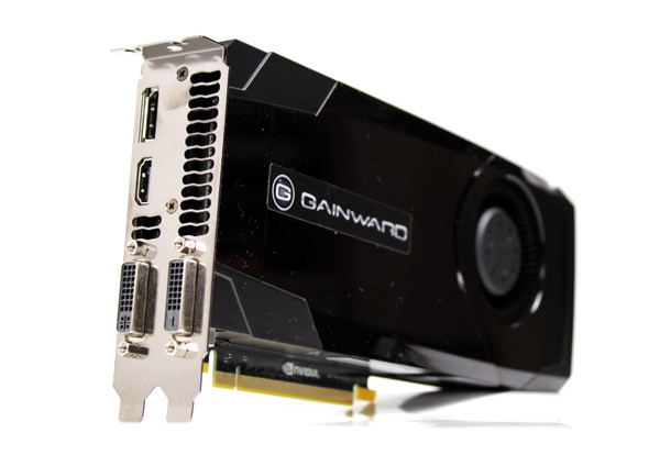
The card is 25,6cm long, whereas last top models like the HD 7970 or GTX 570/580 are 27 long. Just like all high-end cards, Gainward’s GTX 680 allows for chaining up one or two more Geforce GTX 680 cards, in order to get more performance (for 3D Stereo Vision now is enought to have just one GTX 680 graphics card).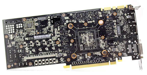
Motherboard: EVGA X79 FTW
CPU: Sandy Bridge-E Core i7 3820 (3.6GHz)
CPU Cooler: Thermalright HR-02 (Thermalright-Europa Distri www.PC-Cooling.de).
Memory: 8GB ADATA DDR3 1600 XPG Gaming series
Harddisk: OCZ Vertex 2 100 GB
Power Supply: CoolerMaster Silent Pro 1000W
Case: CoolerMaster Cosmos II Ultra Tower
Operating System: Win7 64-bit
Nvidia 301.10-desktop-win7-winvista-64bit-english-whql
amd_radeon_hd_7800_8.95.5_win7-64
3DMark 2011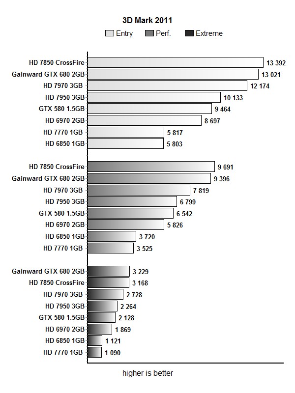
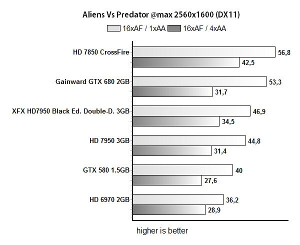
Aliens vs Predator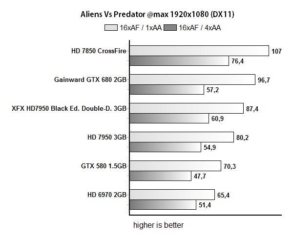
Crysis 2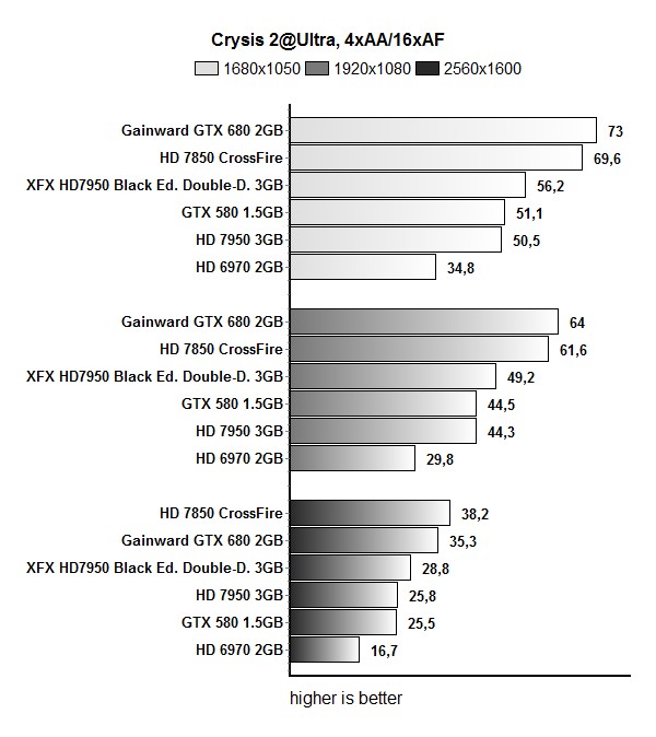
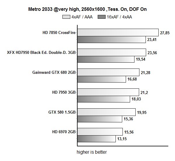
Metro 2033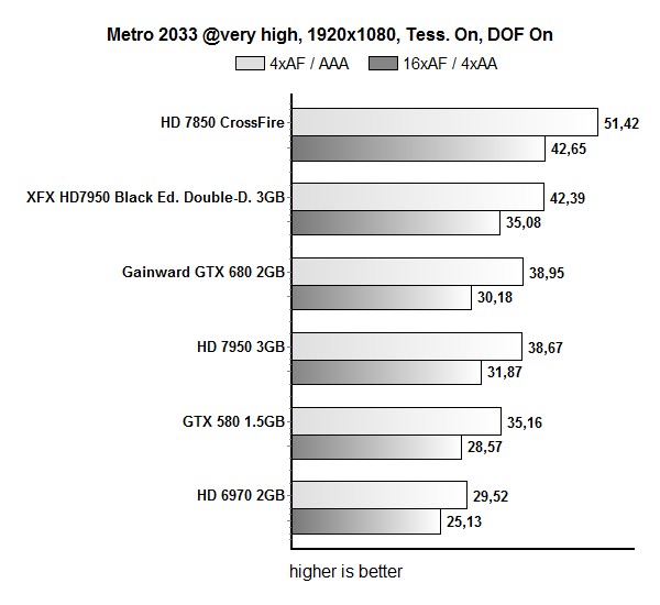
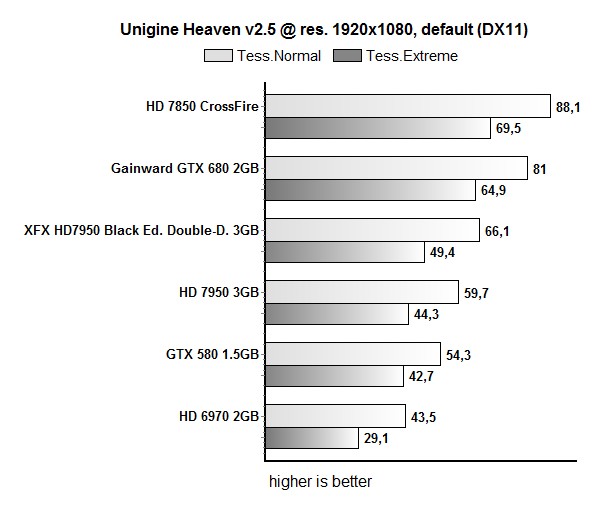
Unigine Heaven
Overclocking and GPU Boost are closely related. Namely, GPU Boost is a hardware implemented feature that cannot be disabled. This feature monitors important operation parameters and calculates optimum GPU clocks. However, although it may seem as an overclocking limiter, overclocking is still flexible enough. In fact, Gainward GTX 680’s OC potential isn’t half bad.
Shader clock is something that Nvidia abandoned with Kepler, but now we have other two clocks worth noting – Base and Boost clocks. Overclocking the GPU within Precision X overclocking tool uses two sliders” “GPU Clock Offset” that affects the Base clock and Boost clock, whereas the “Power Target” slider moves the TDP threshold, which in turn enables higher Base and Boost clocks.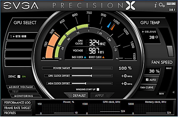
By upping the GPU clock offset, users actually set a new Base clock. This also increases the Boost clock that’s 53MHz higher than the Base clock.
GPU Boost is similar to Intel’s Turbo Boost. If an app or game you started doesn’t overburden the GPU, i.e. doesn’t max out th TDP and thermals, then GPU Boost will up the clock from the Base clock to Boost clock and thus improve performance. Nvidia claims that every GTX 680 is capable of auto-overclocking to Boost clock of 1059MHz. Note however that the clock will still often exceed 1059MHz. The said 1059MHz is the GK104 GPU’s average clock. This is possible because Boost clock is a guaranteed overclock, while maximum clock can even be higher. On our Gainward GTX 680, we measured a maximum clock of 1110MHz.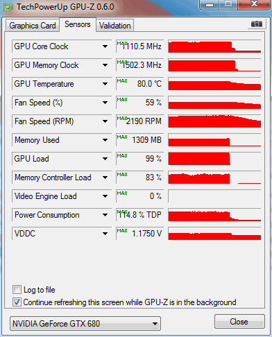
Higher clocks offer the combination of GPU clock offset with Power Target limitation. Nvidia looked at the most demanding games and calculated that the GTX 680’s reference Boost clock has a maximum TDP of 195W (Precision X tool calls this Power Target 100%). By moving the Power Target slider, TDP threshold can be set to 225W (Power Target 132%), which is the most two 6-pin power connectors can offer. This is exactly what we did in our overclocking tests, in order to make sure that the power limit does not limit the desired clock.
Playing Crysis 2 at reference Base clock resulted in 13 different GPU clocks, starting from 1006MHz and ending with 1110MHz (1006/1019/1032/1045/1058/1071/1054/1097/1110MHz). So, overclocking Kepler GPUs won’t provide stable and fixed OC clocks, since the GPU Boost feature produces a range of OC clocks.
Playing at 2560x1600, we noticed that clocks change almost every few seconds, whether it was downclocking or overclocking. Note that the sole exception was 1110MHz as we didn’t see it at this resolution. After we lowered the resolution to 1920x1080 and then 1680x1050, we noticed that clocks remain unchanged longer. In fact, 1280x1024 resulted in almost constant 1097MHz. This clearly shows that GPU Boost gets quite busy when the workload is higher, since it has to intervene and keep the operation parameters within normal limits. This is why it’s difficult to say what’s the maximum clock, because although it can run stable some time, it doesn’t mean it will remain fixed after few hours of gaming.
Our additional “overclocking” resulted in +133MHz offset for the Base clock, i.e. maximum clock of 1230MHz. In average when playing Crysis 2 at 2560x1600 clocks were at and around 1166MHz. The overclocking we’re talking about was done without manual fan RPM setting. The fan isn’t too loud, although it can be heard.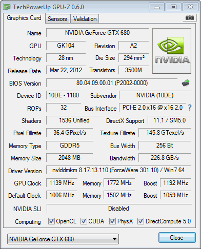
The maximum offset set by Nvidia is +549, so hard core overclockers will have room to play around.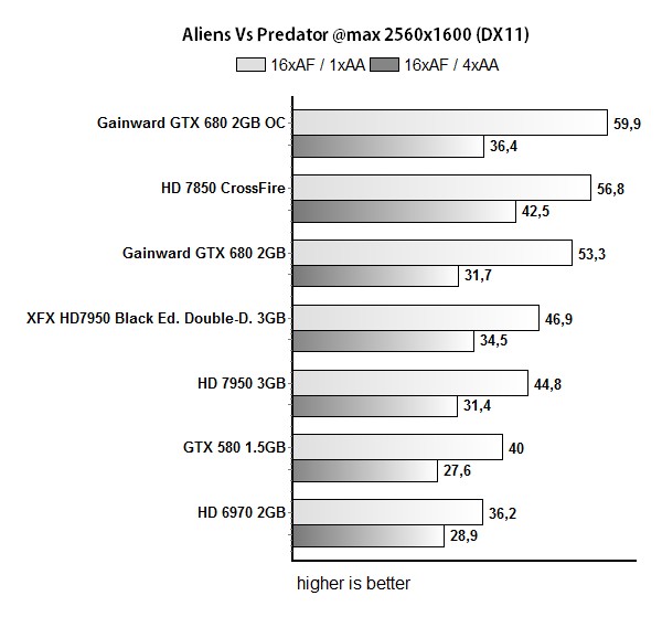
Gainward GTX 680 temperatures go up to 80°C during gaming. Although this may seem a bit high, it’s still good considering the satisfactory noise levels. The GTX 680’s fanproduces a bit more noise compared to GTX 580 ones, but it is still audibly quieter than the HD 7970.
Playing games at reference Base clock (1006MHz) resulted in 13 different GPU clocks, starting from 1006MHz and ending with 1110MHz (Boost clock 1059MHz). Note that there were no sudden changes in fan noise. 
At the same time, 82°C was a stable temperature that allows further overclocking headroom. 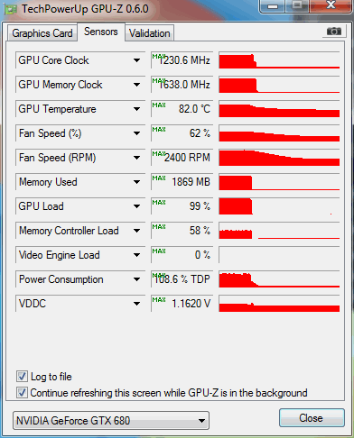
That the cooler is potent was clear from our testing. Namely, we manually sped up the fan to 85% and the temperature dropped from 82°C to 66°C. However, the fan was already too loud at 4000RPM.
Note however the codependency between thermals and clock calculations, which may result in different performance depending on thermals. As soon as the card overheats, which causes current leakage increases, GPU Boost will decrease clocks and voltage. Our additional “overclocking” resulted in +133MHz offset for the Base clock, i.e. maximum clock of 1230MHz, but playing games at 2560x1600 resolution resulted in average clocks at and around 1166MHz.
Power Consumption
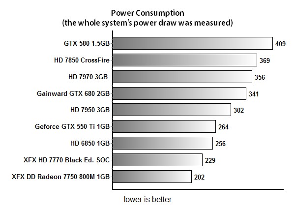
GTX 680’s power consumption is better than that of its main competitor – HD 7970. At the same time, GTX 680 is faster which gives it an edge here. However, AMD’s card boasts ZecoCore, a feature that shuts the card down once the display is off, which slashes consumption to mere 1W. The same scenario will see the GTX 680 consume about 14W. Still, GTX 680’s power management is definitely a job well done because the card scores more than 20% better than its predecessor GTX 580 while consuming 50W+ less.
Gainward’s GTX 680 2GB we tested today is a reference version of the card, but that’s not to say we’re not pleased with its performance. Naturally, we’d much rather try out the Goes Like Hell Golden Sample Edition, because its GK104 GPU and GDDR5 memory indeed pack some overclocking potential, but our today's sample did quite well.
For those who do not like manual overclocking, Nvidia implemented auto-overclocking circuitry within the chip itself and called it GPU Boost. This feature monitors consumption, temperatures and workload, crunches the data and dynamically alters the clocks to provide optimum performance. This is why our Gainward GTX 680 ran at 1110MHz at times. Consumption is monitored by three internal chips, enabling the GK104 GPU to automatically overclock when the card is below the TDP threshold. The GTX 680’s TDP stands at 195W, which is considerably lower than the GTX 580' 244W.
Bottom line is that the GTX 680 is the fastest single-GPU card and provides great performance/consumption ratio. Note however that AMD’s HD 7970 does well at 2560x1600 and matches the GTX 680’s performance in many tests.
Power consumption and the two-display limit were a thorn in Nvidia’s backside for a while now. However, Nvidia finally addressed these issues and the GTX 680 allows for using all four video outs simultaneously.
Currently, AMD's HD 7970 is doing pretty good in Europe. The average price for AMD HD 7970 is around €460, here. Nvidia's GTX 680 is priced at the expected €479, here. The price of GTX 680 will eventually drop in Europe and probably follow the HD 7970 one but, until then, AMD HD 7970 will be doing quite well.
USA, on the other hand, is a bit different. While the EU has seen a slight but constant drop in HD 7970 prices since the launch in December, Newegg.com and other retailers/e-tailers have kept the card at steady US $549.99. Actually, you can currently get it cheaper, for US $534.99, but you have to buy two or more cards, which just a simple deal done by Newegg.com and Sapphire. These prices put AMD in an awkward position in the US, since GTX 680 sells for steady US $499.99.
Gainward’s GTX 680 is a great graphics card for gaming at 2560x1600. Gainward’s GTX 680 is a reference card, but there is little to complain about, since the basic design is nothing short of excellent. The cooling is good, keeping temperatures at bay with relatively little noise, and we have no complaints about the rest of the card either. Since custom designed and overclocked models are nowhere to be found as of yet, Gainward’s card will be a good choice since it’s available and among the most affordable GTX 680s.
Updated:
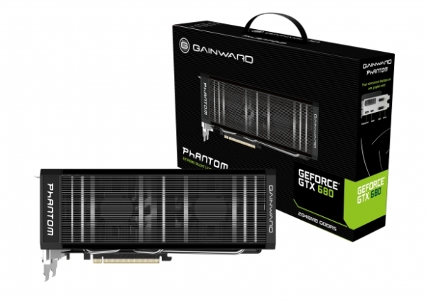
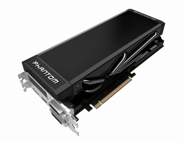
Gainward has now officially launched its newest Geforce GTX 680 Phantom card with custom PCB, factory overclock and new Phantom II cooler.
The new GTX 680 Phantom features a custom PCB with 6-phase DrMOS VRM desing that should provide additional overclocking potential as well more stability. The new GTX 680 Phantom ended up overclocked to 1084MHz for base and 1150MHz for boost clock while 2GB of GDDR5 memory paired up with 256-bit memory interface is working at 1575MHz (6300MHz effective).
The main feature of the GTX 680 Phantom card is its Phantom II cooler. Unlike previous Phantom cooler seen on the GTX 580, this one features new heatsink/fins design that provides better thermal performance, lower acoustic level and more solid structure. We are still looking at a 2.5-slot design with five "grand-prix" 6mm copper-water heatpipes paired up with copper base, large aluminum heatsink and two 80mm silent PWM GR8 fans. All these features add up to provide up to 7.8dB quieter and up to 6°C cooler card when compared to the reference one.
The availability is set for the middle of next month while the price still remains a mystery.
