Index


Review: Faster, cooler, great performer
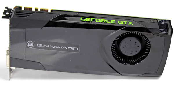
Nvidia launched its first Kepler based card GTX 680 on 22 of March. The goal was pretty much clear – retake some of the ground they lost to AMD. AMD has proudly sat on the single-GPU throne since the 22 of December, when it launched HD 7970 card. It took a lot of effort for Nvidia to achieve this goal, including redesigning the existing architecture to improve performance as well as consumption. The company did a good job and we’ll use Gainward’s GTX 680 as proof. Note that Gainward’s card is only a sticker away from the reference design.
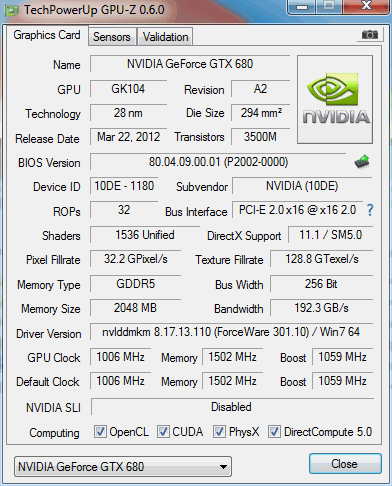
Gainward GTX 680 2GB runs at reference clocks, i.e. 1006MHz GPU and 6008MHz (GDDR5) memory. There are no shader clocks. The difference between Fermi and Kepler architecture lies in the fact that Nvidia equipped Kepler with more shader units. However, these shaders are now slower and run at GPU clocks. So, instead of doubling shader clocks, Kepler comes with double the amount of shaders. Nvidia made sure to boost the GTX 680’s performance and with that in mind, the company not only doubled the GTX 580’s shader count, but tripled it. This means that our today’s card boasts 1536 shader units (or CUDA cores), compared to the 512 units on GTX 580 cards. GK104 was made by TSMC in 28nm and packs 3.54 billion transistors. Note that while this is impressive enough, it’s still not enough to beat the HD 7970’s 4.31 billion. GTX 680 cards come with DX 11.1 and PCI-Express 3.0 support.
One of the things we paid a lot of attention to is the new self-tuning logic, i.e. GPU Boost. This tech fine-tunes clocks on the fly in order to squeeze out maximum juice from the GK104 GPU. The tech runs similarly to Intel’s Turbo Boost. Namely, when the GPU isn’t overloaded and has not exceeded the TDP, GPU Boost will auto-overclock.
Apart from juicing up the performance, Nvidia did a lot of work on power efficiency. You may recall that this was one of the bigger downsides of Nvidia’s last two generations (GTX 500/400), especially when compared to AMD’s offer.


