Index
Review: Great outfit for a gaming party
We like the way EVGA has designed its new GTX 1070 FTW graphics card. It is powerful enough to satisify the most cynical at a gaming party.
The Geforce GTX 1070 is consumer graphics cards which belongs to the new Geforce Pascal generation. While it is the less powerful sibling of the GTX 1080, we think the GTX 1070 is the card for gaming at 1044p. It is just the right card to experience a new class of performance enhanced and VR gaming. When Nvidia unveiled the GTX 1080 earlier this year, it claimed that the GTX 1080 would outperform the GTX Titan X (Maxwell). Now we know the GTX 1070 can do the same thing.
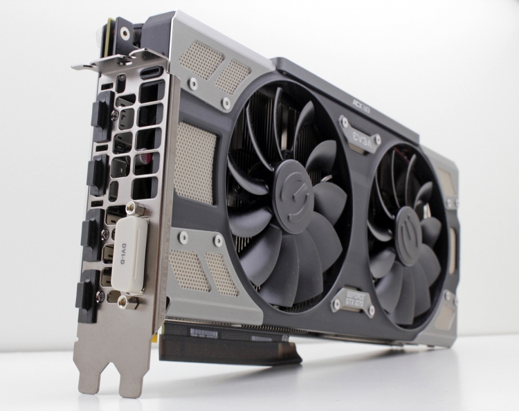
Nvidia has introduced its reference GTX 1070 “Founders Edition”, and its partners are good to go with custom designs. EVGA is one of Nvidia's oldest and most experienced partners and knows how to gain user attention. This time EVGA has two custom coolers for the GTX 1070. The first is based on the new Active Cooling Xtreme (ACX) 3.0 cooler generation, and the second is a hybrid, all in one cooling solution with a maintenance free, self-contained water cooler.
The EVGA GTX 1070 FTW, which we review today, uses the ACX 3.0 cooler. This cooler has many small cool visually appealing details that the best way to present all of them to our readers is through a series of images. Here we show one image of the GTX 1070 FTW card. We left more detailed images and descriptions for the later sections. Please notice that the ACX 3.0 cooler is better than a standard graphics card cooler, but EVGA decided to keep it two slots wide, and you will appreciate this if you decide to go for SLI.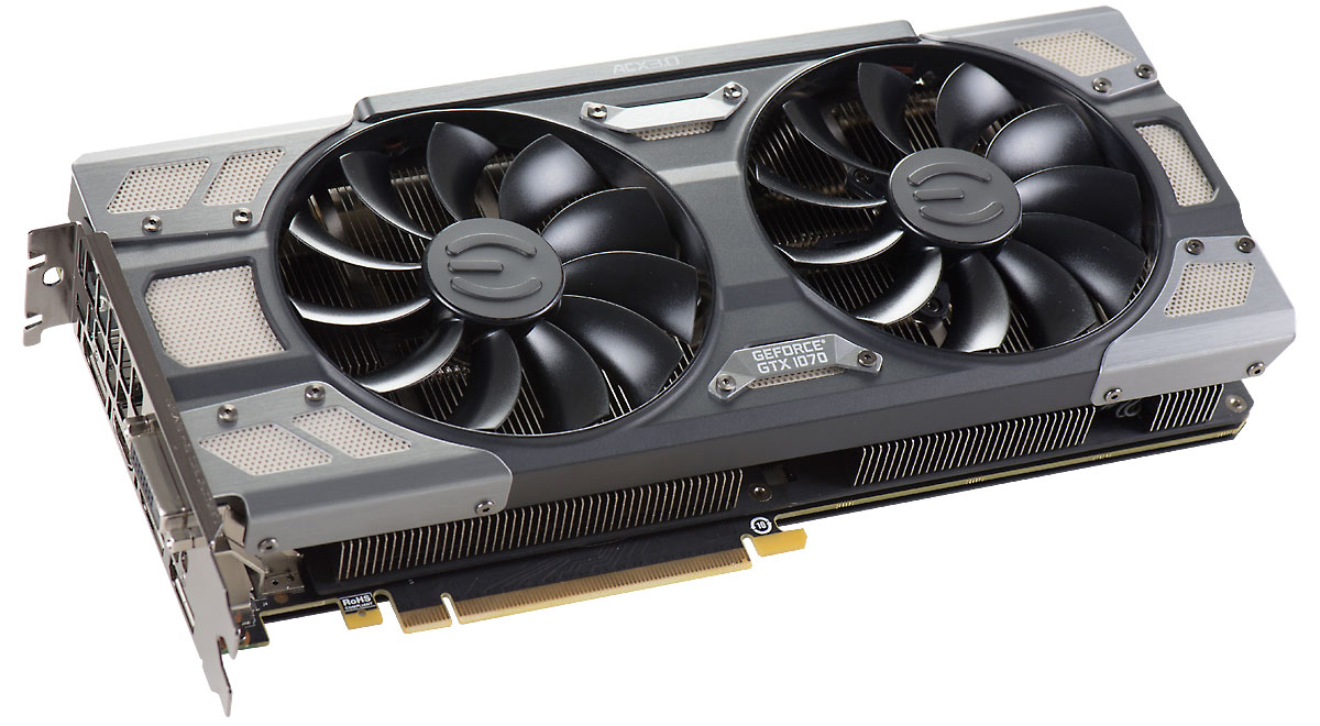
Before we go into detail about FTW card, it is important to compare the GTX 1070 (using GP104 GPU) to its predecessor, the GTX 970 (using GM204 GPU). We will provide some details for the GTX 1080 which is the stronger brother of the GTX 1070. The GTX 1080 and the GTX 1070 are based on the same GP104 GPU, but the GTX 1070 has a lower performance due to some shortcuts through the GPU.
According to technical details, the GTX 1070 isn't a huge improvement on the GTX 970. The important difference is that the GTX 1070 uses the new Pascal architecture. The new Pascal architecture uses TSMC's 16nm FinFET node which is more advanced compared to the 28nm used for the previous Maxwell GM204, and for the GM200 (GTX 980 Ti). By lowering the physical size of transistors it was possible to squeeze 7.2 billion transistors into a 314 mm² package. We are talking here about a fully enabled GP104 GPU which is used on the GTX 1080. With the GTX 1070 some parts of the GPU are disabled Compare this to the 5.2 billion transistors packed into 398 mm² for the GM204. This means the GP104 has 22.9 million transistors per mm2, compared to only 13.1 million transistors per mm² for the GM204.
There are optimisations and improvements across the GPU that provide a better performance per watt. As in the previous generation, the GPU core is divided into four graphics processing clusters (GPC), but the GP104 GPU has less shared resources and more dedicated resources which leads to better performance. While the GTX 1080 comes equipped with a full GP104 GPU consisting of 20 Streaming Multiprocessor (SM) across four GPCs, the GTX 1070 sports only 15 SMs. In other words it has three functional graphics processing clusters.
The GTX 1080 has 2560 CUDA cores vs. 1920 CUDA cores for the GTX 1070, and more TMUs (160 vs. 120). Compare this to the GTX 980 with its 2048 CUDA cores and 128 TMUs. The ALUs design is unchanged. There are still 128 CUDA cores per (SM) and data throughput per clock of this unit is the same as the Maxwell generation. Now there are five SMs per GPC instead of the previous four SMs per GPC. Image below shows the full GP104 GPU.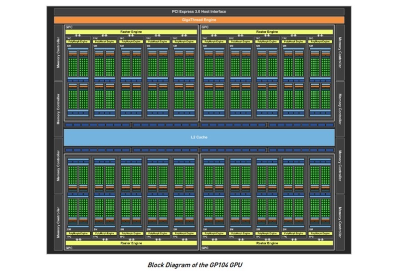
The GTX 1070 uses the same 64 ROPs as the GTX 1080. This number comes from the fact the chip's back end has eight 32-bit memory controllers with eight ROPs and 256KB of L2 cache bound to each. The two graphics cards have the same memory capacity at 8GB. This means memory has been increased compared to 4GB on the GTX 980 and GTX 970. The GTX 1070 uses GDDR5 memory, unlike the GTX 1080 that comes with GDDR5X memory. This affects memory bandwith which is 320GB/s for the GTX 1080 and a nice round 256GB/s for the GTX 1070. This is still 14 per cent higher than GTX 980 with 224GB/s. GDDR5X memory is a new generation of RAM that’s much faster, but it's more expensive than GDDR5.
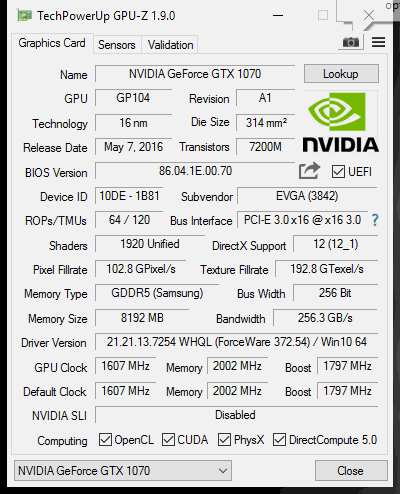
GPU clock is unfortunately detuned for the GTX 1070. For the GTX 1080 Nvidia dialed the GPU's base clock to 1607MHz, while the boost clock is set to 1733MHz. For the GTX 1070 the GPU base clock is set to 1506MHz and its specified GPU Boost clock is 1683MHz.
EVGA GTX 1070 FTW graphics card used in this review had a hefty factory overclock which sets the base GPU clock to 1607MHz, which is as high as the base clock of the more powerful GTX 1080 graphics card. The memory clock is not increased from the reference 8008MHz, which is unfortunate, but EVGA never overclocks memory.