Index
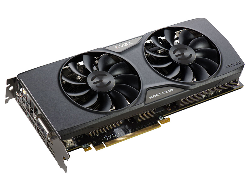
A closer look at EVGA FTW
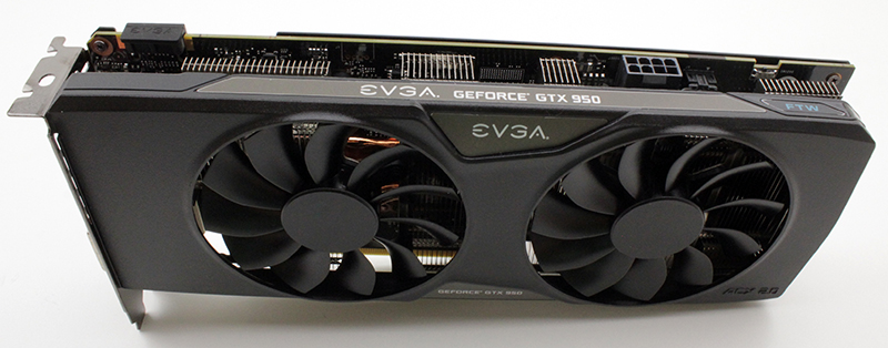
The dual-slot ACX 2.0 cooler looks like it should have no trouble keeping the temperatures and noise emissions in check despite a high factory overclock. The GTX 950 FTW comes with 179MHz GPU overclock, but the GM206 GPU is small chip and it has only 90W TDP. We had a chance to test the ACX 2.0 cooler on the GTX 960 SSC and it impressed us with its low noise. We expect to see better performance on the less powerful GTX 950 FTW.
We’re talking about a dual-slot cooler with two 8.8cm fans on top. The Power Logic PLA09215B12H fan has some good features. It was chosen due to its dense, curved blade design and double ball bearing design.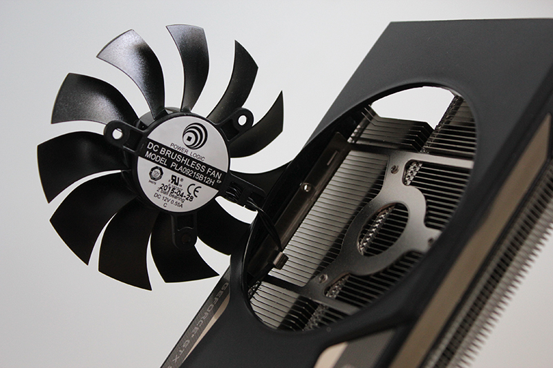
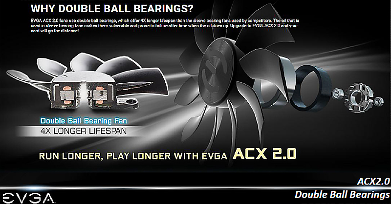
Poor blade design makes more noise but, this 9-blade fan is up to the job. EVGA says the blades are up to 700 per cent more rigid than fan blades in competing fans. This results in a 25 per cent weight decrease. These fans do live up to these claims. The fan uses a double ball bearing design. The noise produced by ball bearing designs is low, at least while they are new. As this fan uses two ball bearings it should last a bit longer and produce a less noise even after a couple of years of wear.
EVGA took an open shroud approach, where fans are positioned on top and blow directly at the heatsink. This approach means that hot air will not be vented from the chassis. Satisfactory airflow ensures the best possible cooling, but it’s nothing that a few quality intake and outtake fans won’t effectively nullify.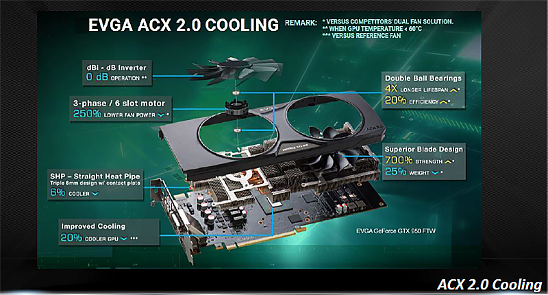
EVGA designed a special heatsink with many dissipation surfaces. Unfortunately you cannot remove the shroud from the heatsink, like on the image above. This is due to a hidden screw below the EVGA Geforce GTX 950 top label. EVGA should remove or reposition this screw and allow the user to remove the shroud easily. On the GTX 980 Ti Superclocked that we tested recently, top label as well as the FTW sign will light once the card is in use. There is no such fancy feature on the GTX 950 cards.
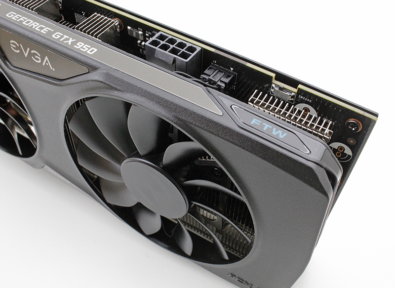
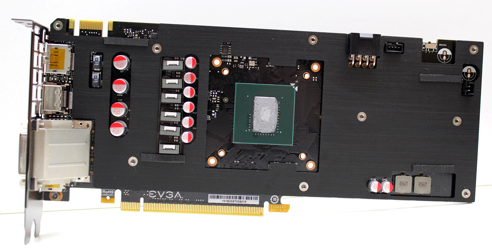
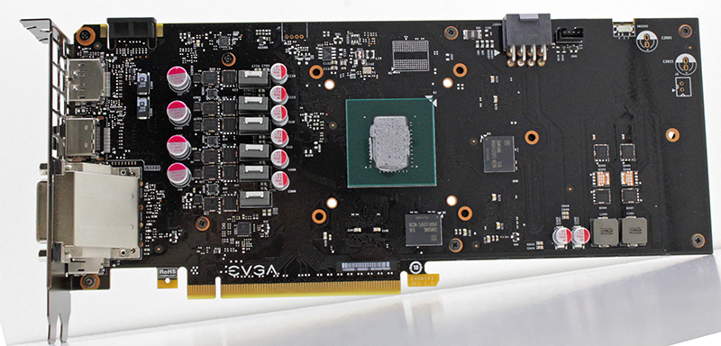
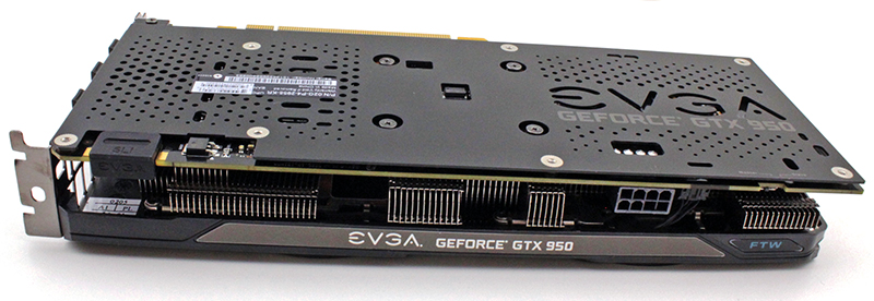
All the juice the card needs can be supplied via the PCIe connector (up to 75W) and one 6-pin power connector (up to 75W). Instead of 6-pin power connector EVGA used an 8-pin power connector (up to 150W). This is not necessary for the card with TDP of 90W, but EVGA used existing PCB and cooler designed for the GTX 960. There is no difference in real life between the two different connectors in a context of the GTX 950.
While it is not a high-end product, Nvidia still enabled SLI support on the GTX 950. With the GTX 750 Ti and GTX 650 Ti SLI this was impossible. It was supported on the GTX 650 Ti boost).
The GTX 950’s display engine supports up to four simultaneous displays at up to 5K (5120x3200) resolution or five physical displays in total. Display outputs include dual-link DVI, HDMI and DisplayPort connectors, with the number varying depending on Nvidia board partners. EVGA GTX 950 FTW comes with one dual-link DVI, one HDMI and three DisplayPort connectors. With support for HDMI 2.0, the Geforce GTX 950 can playback 4K content at 60 fps and it natively supports H.265 (HEVC) encode and decode in hardware. Protective caps are on all video out connectors.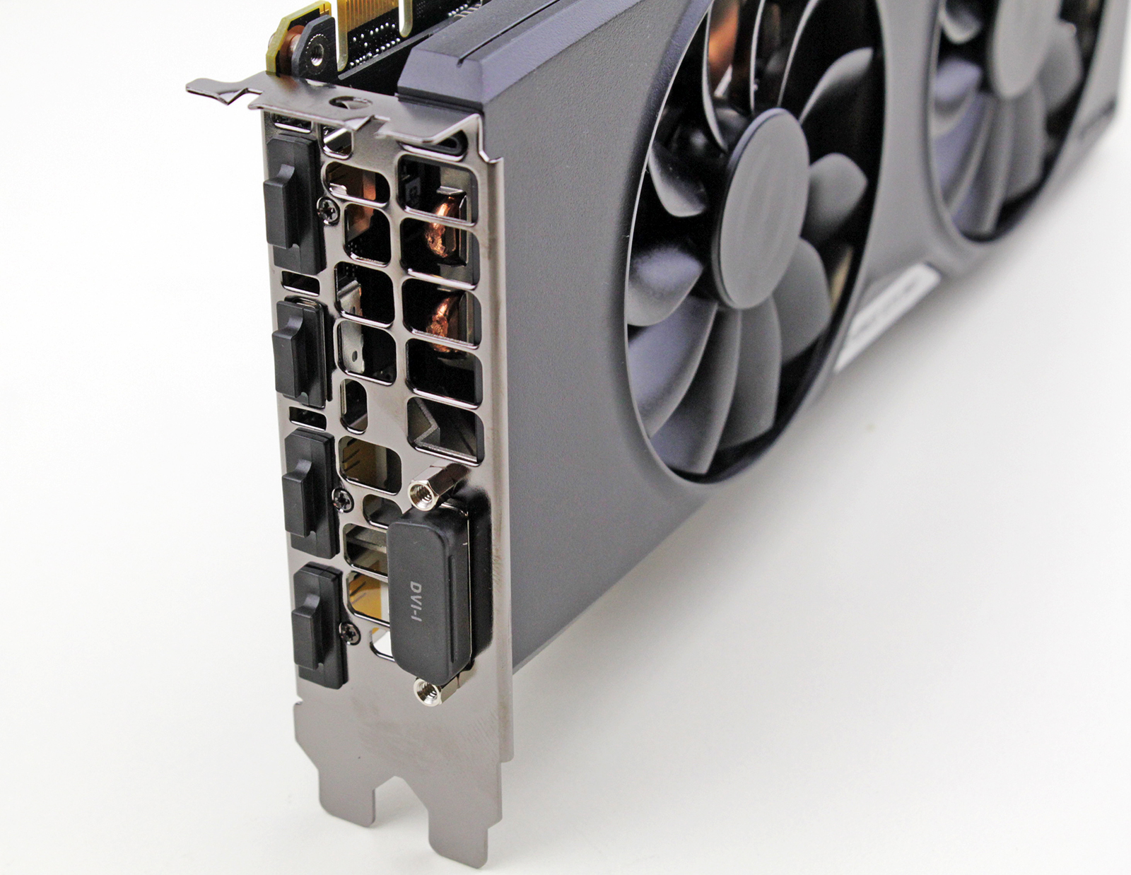
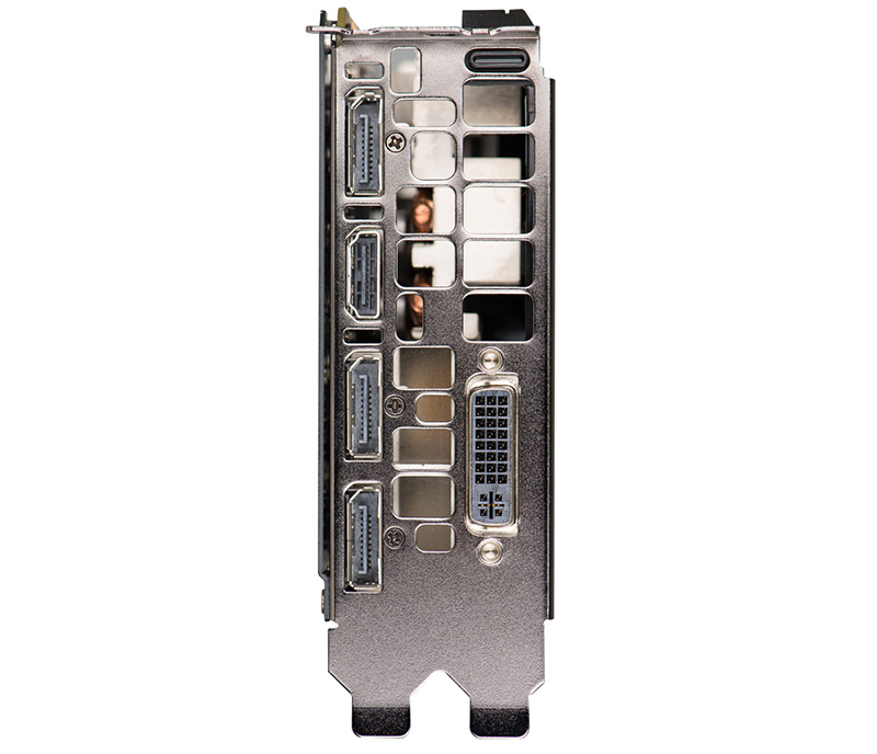
The I/O bracket doubles as an exhaust vent, helping reduce temperatures in the chassis.
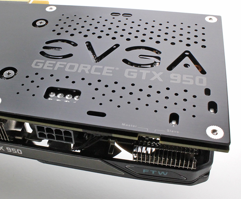
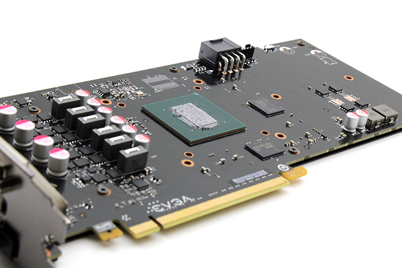
The card has 2GB of GDDR5 memory, courtesy of Samsung. The chip designation is K4G41325FC-HC28. Two of four memory modules are placed on the back side of the PCB where they are covered by nice-looking backplate.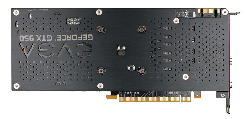
The same memory chips are used on the GTX 970 SSC and GTX 960 SSC. They are specified to run at 1750 MHz (7000 MHz GDDR5 effective) but Nvidia decided to lower the clock down to 1650MHz for the GTX 950.
Compared to GTX 960 lineup of the EVGA cards using ACX 2.0 cooler, the GTX 950 series does not come with full-size cooling plate on the front side of the PCB. You can see how it looks on the image below which shows GTX 960 SuperSC card.
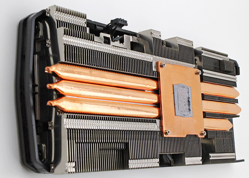
Next image shows the GTX 950 FTW card with the ACX 2.0 cooler removed.
ACX 2.0 cooler on the GTX 950 FTW only deals with heat dissipation from the GPU, while memory and power components are cooled indirectly by airflow.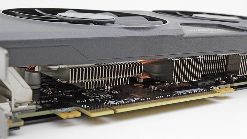
The whole cooler is hold only by four screws in vicinity of the GPU but there are no vibrations or signs of instability.
EVGA designed Straight Heat Pipes (SHP) to reduce the GPU temperature by an extra 5°C. According to EVGA internal testing, the triple 8mm SHP offer 6% better heat dissipation than bent heat pipes with reduced thermal resistance. A big copper base covers the small GM206 GPU.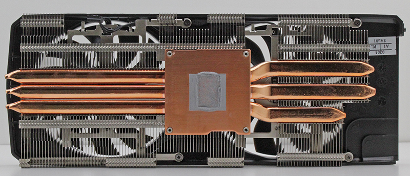
This card is meant for overclocking and QSD (Quick Switch Dual BIOS) allows you to switch to the secondary BIOS with the flick of a switch. The BIOS switch is located close to the PCI power connector. Be aware that changing the vbios does void the warranty, but since the card has a pair of BIOS chips, you can safely modify/flash the slave(secondary) without voiding the warranty.