For TSMC, Q1 2016 was marked by a reduction of demand for high-end smartphones, while smartphone demand in China and emerging markets had upward momentum. Beginning Q2 2016 and onward, the company expect to get back onto a growth trajectory and is projected to hit a 5 to 10 percent growth rate in 2016.
“Our 10-nanometer technology development is on track,” said company president and co-CEO Mark Liu during the company’s Q4 2015 earnings call. “We are currently in intensive yield learning mode in our technology development. Our 256-megabit SRAM is yielding well. We expect to complete process and product qualification and begin customer product tape-outs this quarter.”
“Our 7-nanometer technology development progress is on schedule as well. TSMC's 7 nanometer technology development leverage our 10-nanometer development very effectively. At the same time, TSMC's 7-nanometer offers a substantial density improvement, performance improvement and power reduction from 10-nanometer.
These two technologies, 10-nanometer and 7-nanometer, will cover a very wide range of applications, including application processors for smartphone, high-end networking, advanced graphics, field-programmable gate arrays, game consoles, wearables and other consumer products.”
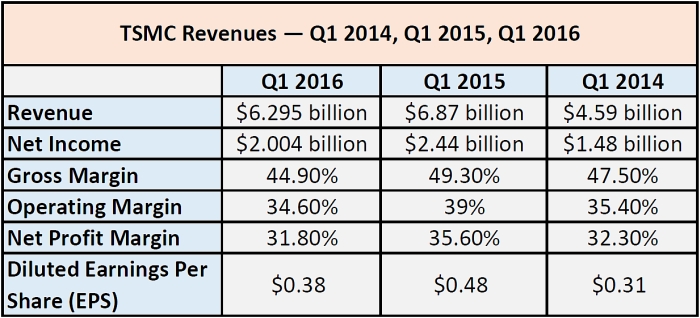
In Q1 2016, TSMC reached a gross margin of 44.9 percent, an operating margin of 34.6 percent and a net profit margin of 31.8 percent respectively. Going forward into Q2 2016, the company is expecting revenue between ~$6.65 billion and ~$6.74 billion USD, gross margins between 49 and 51 percent, and operating profit margins between 38.5 and 40.5 percent, respectively.
TSMC first quarter revenues – 2014, 2015 and 2016
Chips used for communications and industrial uses represented over 80 percent of TSMC’s revenue in FY 2015. The company was also able to improve its margins by increasing 16-nanometer production, and like many other semiconductor companies, is preparing for an expected upswing sometime in 2017.
In February, a 6.4-magnitude earthquake struck southern Taiwan where TSMC’s 12-inch Fab 14 is located, a current site of 16-nanometer production. The company expected to have a manufacturing impact above 1 percent in the region with a slight reduction in wafer shipments for the quarter.
“Although the February 6 earthquake caused some delay in wafer shipments in the first quarter, we saw business upside resulting from demand increases in mid- and low-end smartphone segments and customer inventory restocking,” said Lora Ho, Senior Vice President and Chief Financial Officer of TSMC.
“We expect our business in the second quarter will benefit from continued inventory restocking and recovery of the delayed shipments from the earthquake.”

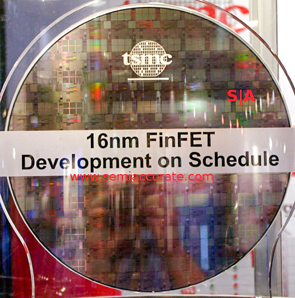
TSMC 16-nanometer FinFET wafer (via SemiAccurate.com)
In fiscal year 2016, the company will spend between $9 and $10 billion on ramping up the 16-nanometer process node, constructing Fab 15 for 12-inch wafers in Nanjing, China, and beginning commercial production of the 10-nanometer FinFET process at this new facility. Samsung and Intel are also expected to start mass production of 10-nanometer products by the end of 2016.
During its Q4 2015 earnings call, company president and co-CEO Mark Liu stated the company is currently preparing and working on a 7-nanometer process node and plans to begin volume production sometime in 2018. Meanwhile, since January 2015, a separate research and development team at TSMC has been laying the groundwork for a 5-nanometer process which the company expects to bring into commercial production sometime in 1H 2020.
So far in Q1 2016, shipments of 16 and 20-nanometer wafers have accounted for around 23 percent of the company’s total wafer revenues.


