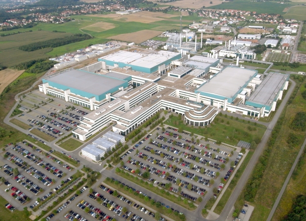
According to Expreview the 14nm process consists of LPE (low-power early) and the LPP (Low Power Plus, advanced low power processing) and both are being churned out at the New York, Malta, Fab 8 wafer fab production.
According to the official disclosure of the progress GloFlo's 14nm LPE process has passed certification earlier this year. Now it appears that yields have reached the level of mass production.
The 14nm LPP process is also underway and expected to be certified in the Q3 quarter and get Quarterly volume production in the first quarter of next year.
, GF 14nm LPP also provides additional functionality, such as an additional IP core, 2.5D and 3D TSV packaging, advanced DFM (design for manufacturability) and better EDA reference flow.
The 14nm LPP system is being pushed towards mobile processors and high-performance core product. This includes AMD next-generation CPU and GPU technology which will use 14nm FinFET technology. Since Gloflo is its old chum it is almost certain that AMD will get them first.
Nvidia
Nvidia might use GloFlo tech in its next generation Tegra processor and GPU .This is just a rumour and besides TSMC is its normal partner, but secretly Nvidia might have hooked up with Samsung.
If this is the case then since GloFlo and Samsung are also allies, it is possible that it could get the work.
Nvidia boss Jen-Hsun Huang, admitted that it was possible but refused to confirm or deny if it was happening.


