They can operate using substantially less electrical charge and are six to ten times faster than silicon, yet due to their incredibly small size they have proven difficult to work with.
The search for silicon alternatives
Over the past 62 years since the first working silicon transistor was made at Bell Labs, companies have used different doping concentrations to influence electron mobility on circuit designs. But over the past half-decade, the industry has been reaching a size limit on how small silicon transistors can be made. Germanium has been considered one possible alternative, as it offers higher electron mobility and is now being used in some CMOS devices.
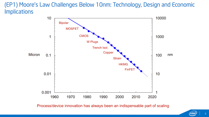
Source: Intel
IBM has built functional silicon-germanium transistors in the 7nm range, but says this node reaches the limits of what can be accomplished with the material. In early 2015, Intel said it would move away from using silicon for its 7nm and later process nodes and will rely on alternative materials that should be available in just over three years. Two materials under consideration have been Indium antimonide (InSb) and Indium gallium arsenide (InGaAs), though Intel has not provided any specific details yet.
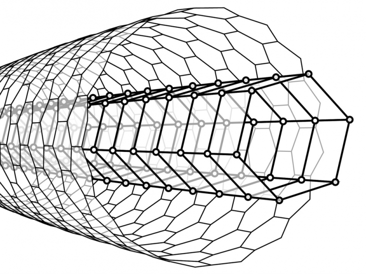
Carbon nanotubes
With any transistor technology, the major hurdles when scaling down are channel and contact size, as smaller nodes can increase electrical resistance between contacts. In October 2012, IBM discovered a solution to resistance issues by creating transistor contacts from the end of each carbon nanotube.
The result was a successfully produced, well-performing carbon nanotube-based chip using 10 thousand transistors at the size of sub-10nm channel lengths. Due to their superior current density at a low operating voltage (0.5 volts), researchers concluded that nanotube-based transistor switching behavior and drain performance was enough to ensure their significance in “future aggressively scaled transistor technologies”.
A change in chip patterning is needed
While most companies are still years away from manufacturing carbon nanotube-based chips on a consumer scale, scientists now realize that the traditional photolithography processes used to pattern CMOS wafers are proving substantially difficult to use with carbon nanotubes due to their small size.
In October 2015, IBM developed a way for CNTs to self-assemble and bind to specialized molecules on a wafer. As IBM Research materials scientists recently George Tulevski told Wired, his team learned how to tackle the problem by borrowing from nature. Instead of placing nanotubes one by one into a desired pattern, the team is treating them with chemicals that allow them to self-assemble into new structures. He says the organic process is “a bit more like growing a crystal than carving a statue”.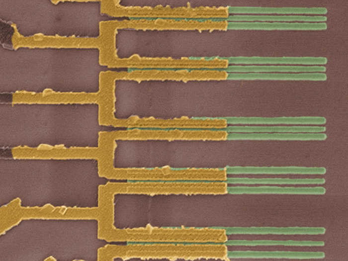
Source: IBM Research
As each tube measures just one nanometer thick and is much less prone to electrostatic discharge, the company concluded they could overcome contact resistance all the way down to an eventual 1.8-nanometer process node in roughly four generations from now.
The promise of opto-electronic chips
To further consolidate space and provide much needed bandwidth, companies have also considered creating new chips that merge electrical and optical properties into a single substrate, or “opto-electronic” chips. In December 2015, a group of researchers from a variety of universities and IBM’s Watson Research Center published a paper called “Single-chip microprocessor that communicates directly using light”.
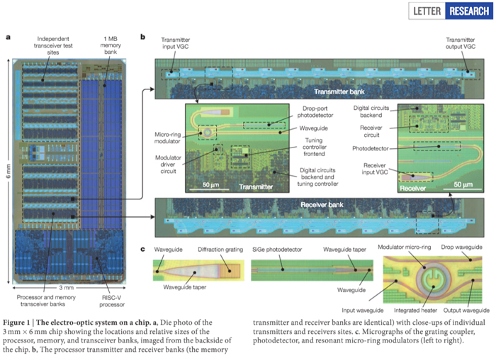
The electro-optic system on a chip - Nature, 2015. DOI: 10.1038/nature16454 (Larger image here)
The dual-core RISC-V design is based on silicon, but it combines over 70 million transistors with 850 photonic components that all together serve processing, memory and interconnect purposes. The CPU and memory components each feature three external optical interfaces – one accepts light from a laser source, a second distributes it to CPU and memory, and the third relays it back. Moreover, the team was able to use a standard CMOS process to design the opto-electronic circuitry.
With silicon’s future prospects dimming, however, there is further research being made on carbon nanotubes to develop PC components with optical interconnects instead of copper. For this to happen at such a nano-scale, however, we are back at the issue of revising chip patterning procedures.
Unfortunately, researchers have not yet discovered how to create one of the key components of opto-eletronic devices, the electrically pumped laser, out of organic material. This is mostly because organic semiconductors have limited charge potential.
On the bright side, carbon nanotubes may have a built-in capacity to generate laser light when exposed to regular light (photon) particles. According to one recent study at the Heidelberg University Institute for Physical Chemistry, there is enough of a strong coupling between carbon nanotubes and light particles that their interaction can generate “laser-like” light emissions, or “quasi-particles” that can serve the purpose of a laser for optical transmission.
Chipmaking cost reductions will be necessary
While the ongoing research for replacing silicon with carbon nanotubes sounds promising, especially with the inclusion of opto-electrical circuitry, the chip manufacturing industry as it stands has already reached a steep cost curve in the move to sub-14nm process nodes.
One of the flip sides to Moore’s Law is Rock’s Law, which observes that the cost of a fabrication plant has doubled every 4 years, with the price reaching about $14 billion as of 2015. Today, the average design cost for a 10nm chip has risen to $120 million plus software fees, while the average cost to design at 7nm scales up to $271 million.
In order for carbon nanotubes, InGaAs, germanium and other alternatives to provide chip makers with an effective Power, Performance and Area (PPA) for their designs, the eventual material must able to significantly bring development costs down if any progress below 7nm is to have any economic advantage.