Index
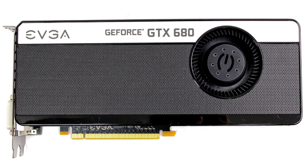
EVGA cools its GTX 670 Superclocked with a blower style fan. The cooler is based on the reference design, although the hood makes it look like a brand new design. In general , the GTX 670 SC is similar to the GTX 680 Signature card we tested here.
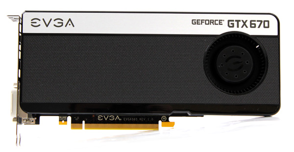
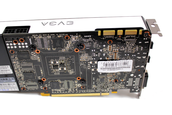
Things get interesting once you flip the GTX 670 over. The PCB ends where the power connectors are but partners are free to implement own designs. In this case, EVGA stuck to the reference design.
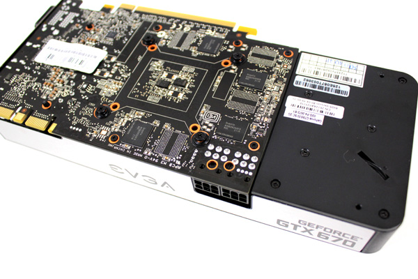
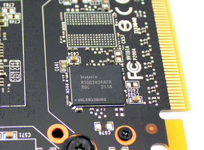
You don’t need to remove cooling in order to see memory modules, or at least half of them. As you can see, the memory chips are placed in a way where every next chip is on the opposite side of the PCB. EVGA’s GTX 670 SC has eight memory chips with 2GB of GDDR5 memory. The card packs eight memory chips totaling at 2GB of GDDR5 memory. Good news for Nvidia fans is that the company kept the identical memory system used on its GTX 680 card, meaning four 64-bit memory controllers (256-bit memory interface) and 2GB of GDDR5 memory. The memory runs at 1502MHz (6008MHz effectively), again just like the GTX 680.
EVGA’s GTX 670 Superclocked runs Hynix memory chips (model No: H5GQ2H24AFR-R0C). The chips are specified to run at 1500MHz (6000MHz GDDR5 effectively). GTX 670 Superclocked’s memory runs at 1552MHz (6208MHz effectively). We’ve seen this same memory on many AMD HD 7970 cards, although it ran significantly slower at 1375MHz. Note however that HD 7970 cards come with 3GB of memory.
The mesh finish on the Superclocked’s cooler looks quite attractive, but closer inspection reveals it’s only a finish on plastic.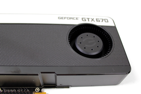
Blower style fan pushes air through the cooler and forces it out. Dual fan coolers are usually the best ones but they tend to leave hot air in the case. Anyhow, you’ll have to have adequate cooling if you want to throw in a GTX 670.
The plastic shroud, which we took off on the picture below, acts as a tunnel for air, channeling it from the fan, across the heatsink and out the I/O panel exhausts.
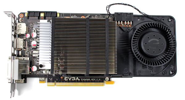
Although the GTX 670 is 24.1cm long, the PCB is only 17.2cm. Nvidia moved the power circuitry from its usual spot at the end of the card. This left empty space at the end of the PCB, so the company simply cut it off and saved on materials.
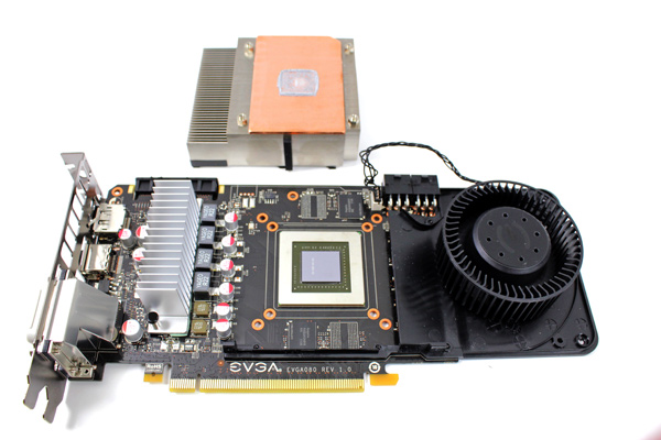
The memory on the PCB side isn’t cooled.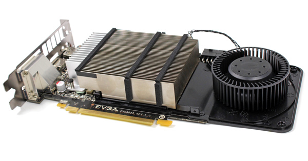
The heatsink is smaller but somewhat resembles the GTX 680’s heatsink (picture below).
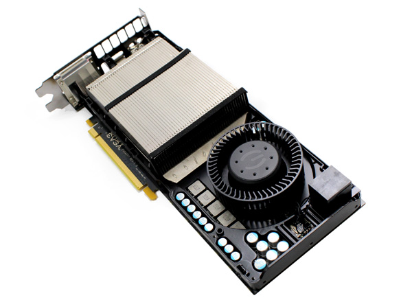
Reference GTX 670 cards draw power via two 6-pin power connectors, just like the factory overclocked EVGA GTX 670 Superclocked. The reference TDP stands at 170W, but you can expect EVGA’s GTX 670 Superclocked to slightly top that due to the overclock.
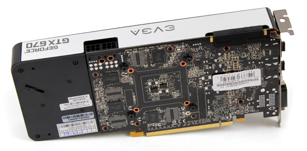
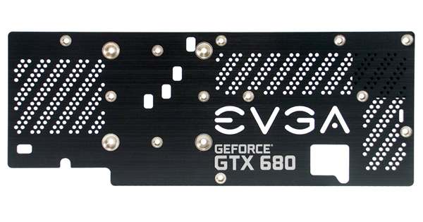
It would be nice if EVGA offered its Backplate for this card, since it does many things. Namely, it makes the card look sweeter, reinforces the PCB and can even passively cool the memory.
The following photo shows how Nvidia did the part where the PCB and cooler meet. The fan is on a separate piece of plastic that’s fixed to the PCB via four screws.
EVGA GTX 680 SC Signature comes with two dual-link DVI outs, but only one is analog VGA-out capable. EVGA made things easy by marking the VGA-capable out with “DVI-I”. The plastic caps are also a nice touch. The I/O panel holds a standard HDMI and standard DisplayPort. Nvidia made sure not to lag behind the competition so Kepler based cards can run up to four displays simultaneously.
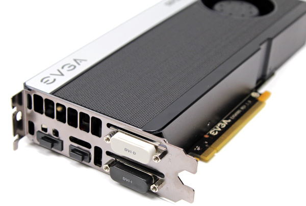
The air exhausts are wider than on the reference card. This allows for easier air movement, which can decrease temperatures by up to 3°C in best case scenarios.
