Index
- Nvidia Geforce GTX 1080 Ti review
- GPU and memory overview
- Specifications, packaging and hardware overview
- Test Setup
- Results – Nvidia Vulkan API demo
- Results – Cinebench R15
- Results – Civilization VI
- Results – Just Cause 3
- Results – No Man's Sky
- Results – Far Cry 4
- Results – 3DMark + Time Spy
- Results – Unigine Heaven 4.0 Benchmark
- Overclocking
- Conclusion
- All Pages
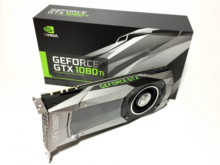
GP102-350
The Geforce GTX 1080 Ti ships with a GP102-350 under the hood, rather than GP102-400 on the Titan X, but features the same number of cores – 3584 – and the same number of texture units – 224. However, the number of ROPs gets decreased from 96 to 88. Each core contains 28 streaming multiprocessors (SMs), and each SM contains four double-precision (DP) units each. To account for the decrease in ROPs, the core clock has been increased to 1480MHz versus 1417MHz on the Titan X, yielding a texture fill rate of 354.4 gigatexels per second, or about a 62 percent increase over the previous flagship card and 85 percent higher than the GTX 980.
Improved memory architecture
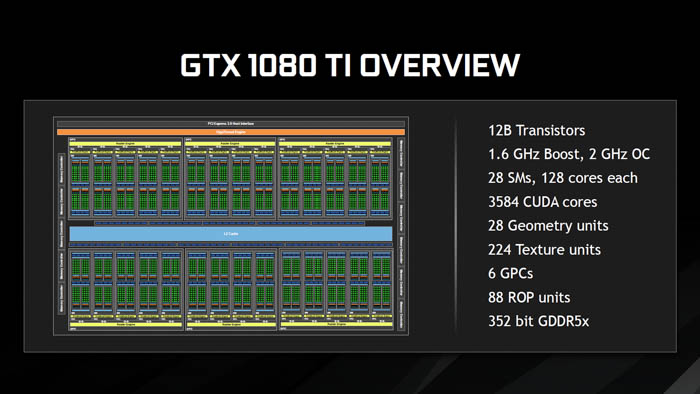
During its press briefing, senior GPU architect Jonah Alben went on stage to discuss the GTX 1080 Ti’s improved memory architecture and how it now uses next-generation GDDR5X modules from Micron running at 11Gbps. This has been achieving using a technique called “advanced equalization” that allows for a "much cleaner signal" consisting of minimal noise, less jitter and less power, temperature and voltage (PVT) loss.
The above image shows two sampled data eye diagrams of the memory interface, where the left image shows the original GDDR5X running at 11Gbps and the right shows the redesigned GDDR5X modules with a much cleaner “data eye.” At this bandwidth speed, the original memory design was not able to separate data values reliably in the center of the image is where the values are sampled. The company was thus able to decrease the bus width from 384-bits on the Titan X Pascal to 352-bits while also gaining a speed increase from 10Gbps to 11Gbps, and peak memory bandwidth increase from 480GB/s to 484GB/s.
Alben explained that most modern GPUs use a technique called “immediate rendering” – you get triangles to come into the scene, transform them, and immediately push them to the back end of the chip. In terms of memory bandwidth, geometry is immediately read through the L2 cache and then processed in DRAM. Alternatively, there is a technique called “tiled rendering” that divides the triangles into large individual tiles that substitute L2 cache for a “tile buffer” that sends several squares at a time in parallel directly to DRAM. The drawback is that this approach has a downside for high-performance gaming because geometry is read, sent back to memory, and then read again. With the goal of reducing bandwidth as much as possible, the tiling approach cannot stand up to the pixel-dense bandwidth requirements of modern content.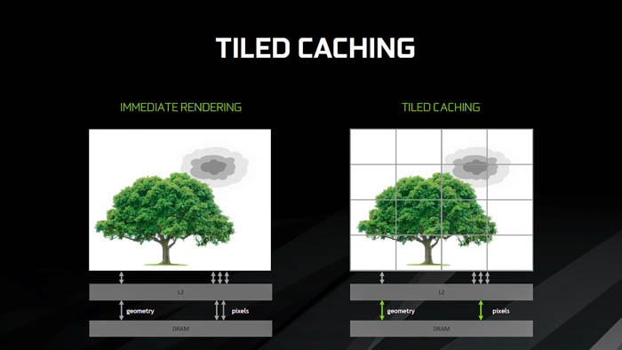
In the previous Maxwell generation, the company’s engineers designed a technique called “tiled caching” to improve cache locality and reduce memory traffic. This approach still renders a single portion of the screen at a time, but now it sends triangles through an on-chip geometry queue called a “binner.” Once this queue fills up, the contents are sent out to the Rasterizer in a tiled way. “In the case where tiling is a bad idea, we don’t use it. When tiling is a good idea, we use it.”
Nvidia says that tiled caching can be described as an enhancement “intermediate architecture” that doesn’t pay the latency tax of having to go through memory multiple times in a single rendering process. The technique uses L2 cache coherency, which is another way of saying that the contents of multiple caches remain together and consistent. On the front-end, there is no difference in the geometry processing – all of the reductions in pixel bandwidth are now done on the back-end, and this is where pixels will stay until the rendering is complete.
In terms of raw memory performance with a redesigned GDDR5X controller, the GTX 1080 Ti is able to surpass HBM2’s peak bandwidth-per-package rate of 256GB/s by about 64 percent, to 400GB/s. Using compression techniques alone, Nvidia is able to increase the amount of memory bandwidth from 400GB/s to 900GB/s, or about 2.25 times. By combining compression with tiled caching, it can now bring that 900GB/s number all the way up to 1200GB/s, or another 30 percent.
Framebuffer requirements now being met for most premium displays
In 2014, the average size of the VRAM framebuffer at the introduction of some of the first 4K-ready graphics cards was between 3.5GB and 4GB. Most 1080p titles only required 2GB at most, while titles such as GTA V running at 1440p required around 3.5GB. As ultra-wide 21:9 monitors came into mainstream retail channels, this requirement soon increased to 5.27GB, while 4K and 5K have pushed the numbers up to 7.91GB and 14.06GB, respectively.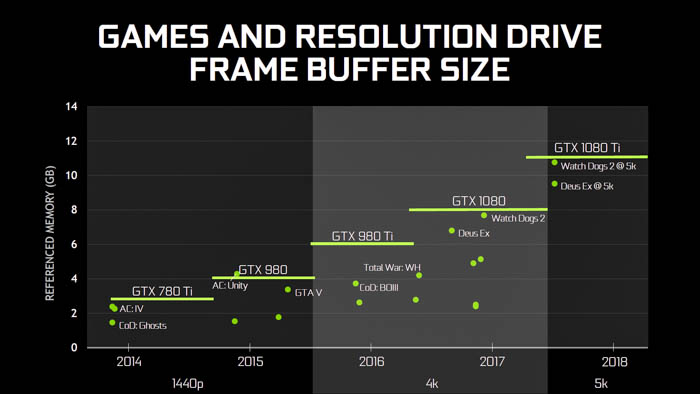
Two years ago, the Maxwell-based Titan X became the first consumer card to feature a 12GB framebuffer, meeting the requirements for most displays in UHD resolution and above. AMD soon realized the importance of meeting these framebuffer requirements and introduced the Radeon R9 390 and 390X the following summer with 8GB of GDDR5 memory each. Nvidia’s lineup was refreshed by the Pascal-based Titan X with 12GB of GDDR5X, along with the GTX 1070 and GTX 1080 with 8GB of GDDR5 and GDDR5X, while AMD followed up with Polaris-based Radeon RX 470 and 480X featuring 8GB of GDDR5 each, respectively.
Now in Q1 2017, the company has decided that it will take the 12GB GDDR5X framebuffer previously only available in its $999 to $1200 flagship Titan X series, and offer it to a larger customer base thanks to the lower $699 point of the Geforce GTX 1080 Ti. Not only will the capacity for more pixel transfer be increased, but the speed of data has also been optimized to 11Gbps at the lower effective price point, making this card a more ideal way to save on the purchase price of these new premium UHD displays.