Index
Overclocking and GPU Boost are closely related. Namely, GPU Boost is a hardware implemented feature that cannot be disabled. This feature monitors important operation parameters and calculates optimum GPU clocks. However, although it may seem as an overclocking limiter, overclocking is still flexible enough. In fact, Gainward GTX 680’s OC potential isn’t half bad.
Shader clock is something that Nvidia abandoned with Kepler, but now we have other two clocks worth noting – Base and Boost clocks. Overclocking the GPU within Precision X overclocking tool uses two sliders” “GPU Clock Offset” that affects the Base clock and Boost clock, whereas the “Power Target” slider moves the TDP threshold, which in turn enables higher Base and Boost clocks.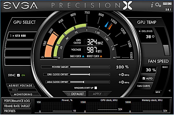
By upping the GPU clock offset, users actually set a new Base clock. This also increases the Boost clock that’s 53MHz higher than the Base clock.
GPU Boost is similar to Intel’s Turbo Boost. If an app or game you started doesn’t overburden the GPU, i.e. doesn’t max out th TDP and thermals, then GPU Boost will up the clock from the Base clock to Boost clock and thus improve performance. Nvidia claims that every GTX 680 is capable of auto-overclocking to Boost clock of 1059MHz. Note however that the clock will still often exceed 1059MHz. The said 1059MHz is the GK104 GPU’s average clock. This is possible because Boost clock is a guaranteed overclock, while maximum clock can even be higher. On our Gainward GTX 680, we measured a maximum clock of 1110MHz.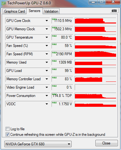
Higher clocks offer the combination of GPU clock offset with Power Target limitation. Nvidia looked at the most demanding games and calculated that the GTX 680’s reference Boost clock has a maximum TDP of 195W (Precision X tool calls this Power Target 100%). By moving the Power Target slider, TDP threshold can be set to 225W (Power Target 132%), which is the most two 6-pin power connectors can offer. This is exactly what we did in our overclocking tests, in order to make sure that the power limit does not limit the desired clock.
Playing Crysis 2 at reference Base clock resulted in 13 different GPU clocks, starting from 1006MHz and ending with 1110MHz (1006/1019/1032/1045/1058/1071/1054/1097/1110MHz). So, overclocking Kepler GPUs won’t provide stable and fixed OC clocks, since the GPU Boost feature produces a range of OC clocks.
Playing at 2560x1600, we noticed that clocks change almost every few seconds, whether it was downclocking or overclocking. Note that the sole exception was 1110MHz as we didn’t see it at this resolution. After we lowered the resolution to 1920x1080 and then 1680x1050, we noticed that clocks remain unchanged longer. In fact, 1280x1024 resulted in almost constant 1097MHz. This clearly shows that GPU Boost gets quite busy when the workload is higher, since it has to intervene and keep the operation parameters within normal limits. This is why it’s difficult to say what’s the maximum clock, because although it can run stable some time, it doesn’t mean it will remain fixed after few hours of gaming.
Our additional “overclocking” resulted in +133MHz offset for the Base clock, i.e. maximum clock of 1230MHz. In average when playing Crysis 2 at 2560x1600 clocks were at and around 1166MHz. The overclocking we’re talking about was done without manual fan RPM setting. The fan isn’t too loud, although it can be heard.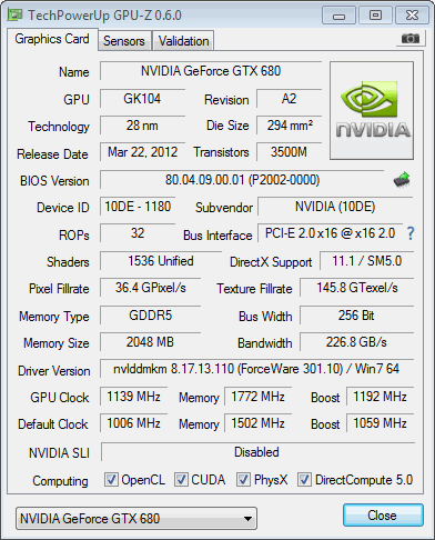
The maximum offset set by Nvidia is +549, so hard core overclockers will have room to play around.