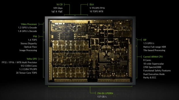
We have heard this pitch before, and it has happened so many times in Nvidia history that we witnessed that two-week-old silicon was up and running and working fine. This is a very unlikely case in SoC engineering but hey, that is what the Nvidia CEO said to the hundreds of people at the press conference. Nvidia's CEO promised back in September 28 2016 that Xavier will be shipping to Tier one OEMs in Q4, and now it seems that it has slightly slipped to Q1 2018.
Xavier is big, and it might be the biggest SoC that we ever seen. Jensen held it in his hand and mentioned that this SoC has nine billion transistors. Snapdragon 835 has three billion transistors and it is the best thing for mobile shown in 2017. It is 350 square mm which is huge for an ARM-based SOC. It becomes clear that Xavier won't be in any mobile and tablet devices, this is an automotive solution only.
350 square nm automotive
Xavier is 350mm square and a 12nm processor manufactured at TSMC and Jensen claims that it took 8,000 engineering years and billions of dollars to get Xavier up and running.
Nvidia is using a fully customised ARM64 Carmel core with 10 wide superscalar, 2700 spectInt 2000, functional safety features, dual executing mode parity and ECC. Of course, this is an eight core CPU.
Nvidia uses Volta GPU, FB 32/ FP16 / FP8 multi precision, 512 Cuda cores, 1.3 Cuda Teraflops and 20 tensor cores TOPS. This gives you an idea that Volta comes hand in hand with tensor cores and tensor cores are a waste of silicon for graphics and gaming. In other words, there is something other than Volta for GPUs coming later in 2018.
Volta meets Deep learning
Nvidia has DLA Deep learning assistant as part of the chip, scoring 5Tflops FP16 and 10 Tflops FP8. It supports 16 CSI, a camera interfaces capable of 109 Gbps supporting 1gE and 10 Gigabit Ethernet for all the in-car cameras. Xavier is level 3 and level 4 autonomous solution with some 30ish W TDP.
It also supports 1.2 Gpix / Encode and 1.8 Gpix / Decode capable audio processor. Xavier supports 256 Bit LPDDR4 with 137 GB/s speeds. The last part of the chip detailed is PVA and we don’t know what PVA stands for. Maybe someone will come up with an idea in our comment sections.
The PVA is 1.6 Tera operations per second, with stereo disparity, optical flow, and image processing.
The actual shipping of this processor will come much later in 2018 and it will take a while since can to buy a car based on it, but this is an important milestone and probably the most powerful automotive solution around.


