

Samsung’s 3nm process is the industry’s first commercial production process node using gate-all-around transistor (GAAFET) technology, so the announcement is a major milestone for the field of silicon lithography.
The company is not disclosing the specific version of the node used here, but this is likely to be the initial 3GAE process. According to Samsung, the line will initially be used to produce chips for “high performance, low power computing”, with mobile processors to come later. Early process nodes are reserved for the company’s internal use so we are not seeing any 3nm chips but it is only a matter of time.
The outfit has been so quiet about the new process launch there had been more than some concern that 3GAE would be delayed past 2022 but today's announcement means that everything is on time.
![]()
That said, Samsung’s announcement leaves the company with a fair bit of room with regards to just how many chips they’re capable of producing, what yields and when they will be with us. The company was producing test chips back in 2021 so everything should be a bit clearer particularly since Samsung has been working on 3nm/GAAFET technology since before 2019.
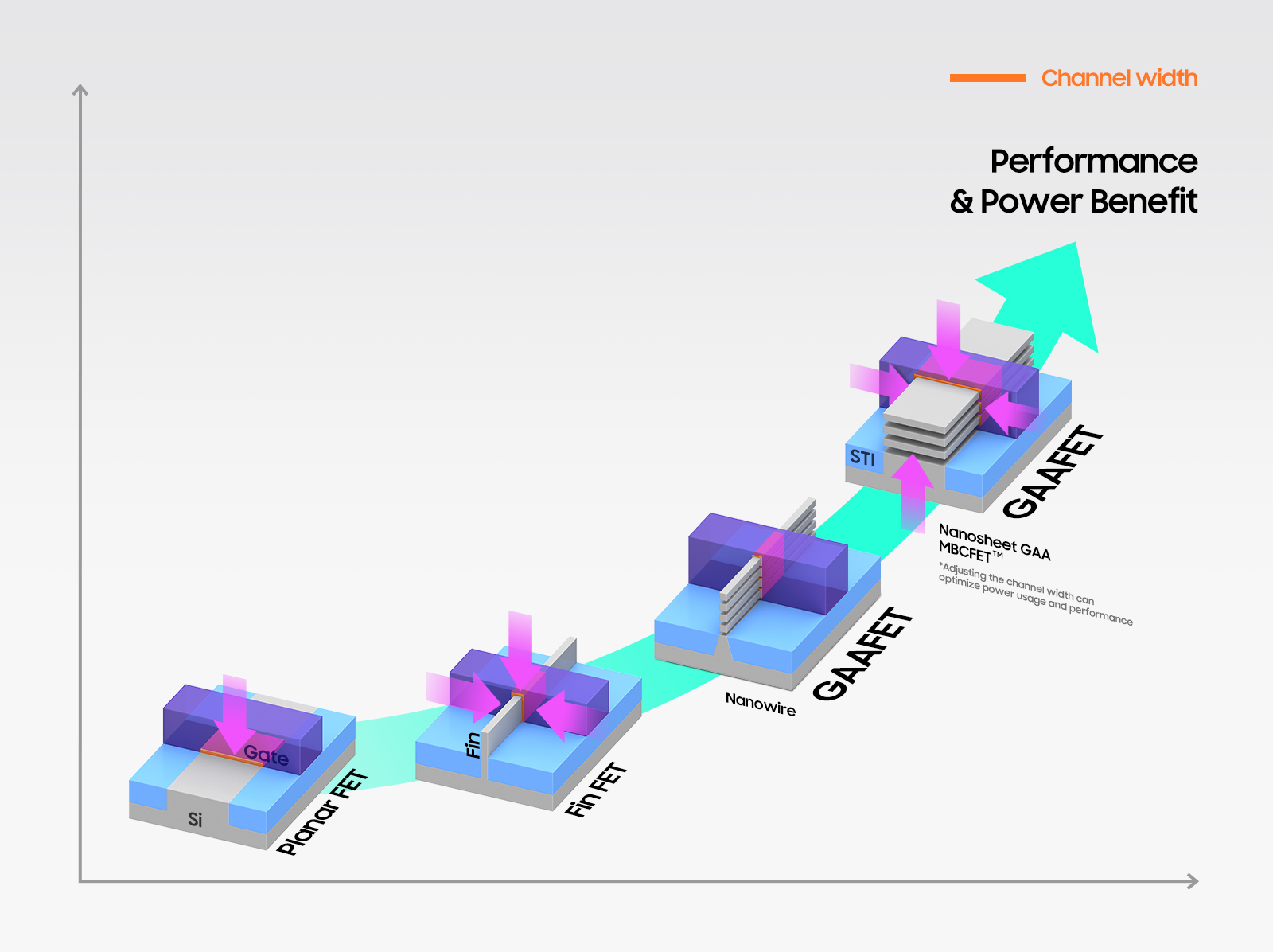
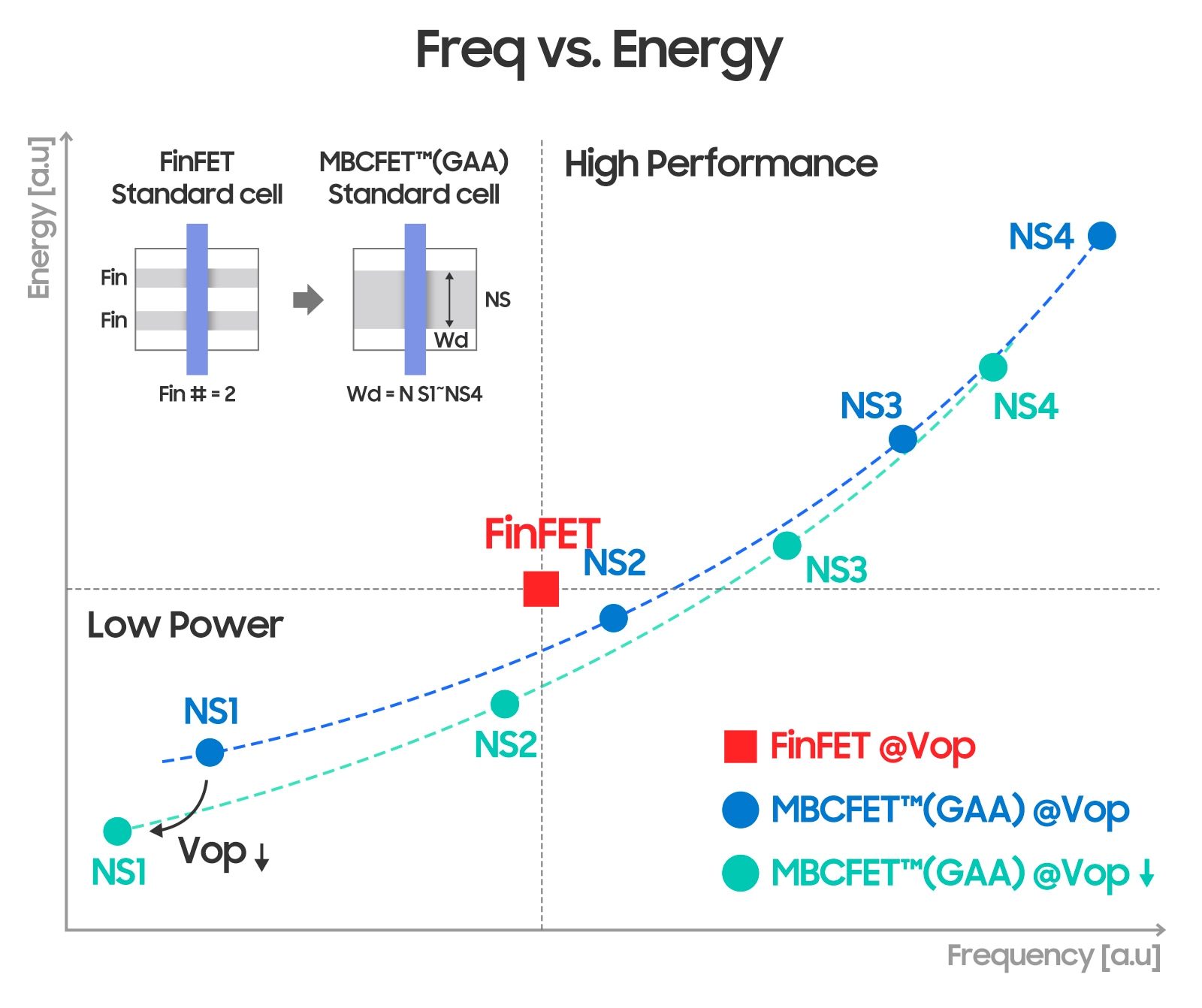
Samsung’s uses GAA transistor technology is Multi Bridge Channel FET (MBCFET), which is a nanosheet-based implementation. Nanosheet-based FETs are extremely customisable, and the width of the nanosheet is a key metric in defining the power and performance characteristics: the higher the width, the higher the performance (at higher power). As a result, transistor designs that focus on low power can use smaller nanosheets, while logic that requires higher performance can go for the wider sheets.
Samsung has also offered some updated size and performance figures comparing 3GAE to older nodes. Officially, 3GAE can offer 45 per cent reduced power consumption or 23 per cent improved performance compared to Samsung’s 5nm process (the company doesn’t state which flavor), with an overall reduction in feature size of 16 per cent. These figures are notably different from Samsung’s previous (2019) figures, which compared the tech to Samsung’s 7LPP node. Given the change in baselines, it’s not clear at this point whether 3GAE is living up to Samsung’s initial claims, or if they’ve had to back off a bit for the initial version of their 3nm technology.
According to today’s press release, Samsung is expecting a 50 per cent power reduction or 30 per cent performance improvement versus the same 5nm baseline, with a much greater 35 per cent area reduction.


