Fudzilla readers will be familiar with TSMC but for people searching for this, every iPhone, most Qualcomm Snapdragon’s, AMD’s 7nm Ryzen, EPYC, Radeon as well as Geforce / Tesla / Quadro are made there. For the record, TSMC stands for Taiwan Semiconductor Manufacturing Company.
Godfrey Cheng, who recently joined as the head of global marketing, wrote a nice blog on his vision of Moore’s Law. There has been a lot of discussion about how the "Law" is dead and how doubling the number of transistors every two years id history.
TSMC has a solution for its continuation as Godfrey concludes that instead of chasing the frequency and increasing the single transistor performance, the solution is in higher density. Industry opponents to Moore’s Law claim that you cannot continue to shrink the transistors any further and that there will be physical limitations.
To refresh your memory, Intel was stuck at 14nm for a few generations and now finally managed to get to 10nm while companies like Apple and Qualcomm, who are at the leading-edge technology for its phone chips used 10nm in 2017 / 2018 phones and 7nm in 2018/2019 or current generation phones.
To continue putting billions of chips on a very small 2D area, it was logical that after 7nm comes 5nm and so on. Apple’s 7nm A12 chip inside of the iPhone Xs has 6.9 billion transistors on the 83.27 mm2 area.
TSMC solution for the continuation of Moore’s Law
The solution called N5P is a process developed by the company to bring customers highest possible density with the best performance. Today's workloads revolve around CPU, GPU related tasks and are heavily influenced by the enormous need for computation for the existing and the future AI workloads.
One of the big obstacles is to feed the CPU/GPU or an integrated circuit or SoC with enough data. The parallel processor is only good if the interconnect and memory interface can keep all the pipes busy and fed.
TSMC sees a solution in massive interposer and advanced packaging techniques. A few recent examples familiar to readers involve AMD Vega, Nvidia Tesla, and Xilinx Versal chips, all having the HBM 2 memory on the interposer. It is no coincidence that all of the above products are manufactured at TSMC.
Having memory on the same package as the CPU/GPU speeds up computation as the pipelines are getting the data at much higher speeds compared to traditional memory. HBM 2 supports speeds up to 460 GB/s with some products and Radeon VII, or Vega 20 has a total bandwidth of 1028 GB/s manufactured on TSMC’s 7FF (Fin Fet) process. Nvidia’s V100 Volta-based Tesla compute AI card has a total bandwidth of 900 GB/s, and any GPU/AI company wants even more bandwidth than that.
Godfrey is teasing the N5P node, and TSMC will likely give us a bit more details at the Hotchips Conference starting Tuesday, August 20 in the keynote session named “What Will the Next Node Offer Us?” by Dr. Philip Wong, VP Corporate Research, TSMC.
TSMC’s first shot at 5nm called N5 process started risk production in March 2019 and compared to N7 7nm volume production the N5 offers 80 percent more density, 15 percent more speed and 30 percent less power. The new eLVT transistors can offer speed gains as high as 25 percent.
The new N5P that is expected to enter the risk production next year should squeeze an additional seven percent in speed and 15 percent in power compared to N5.
System-level innovation
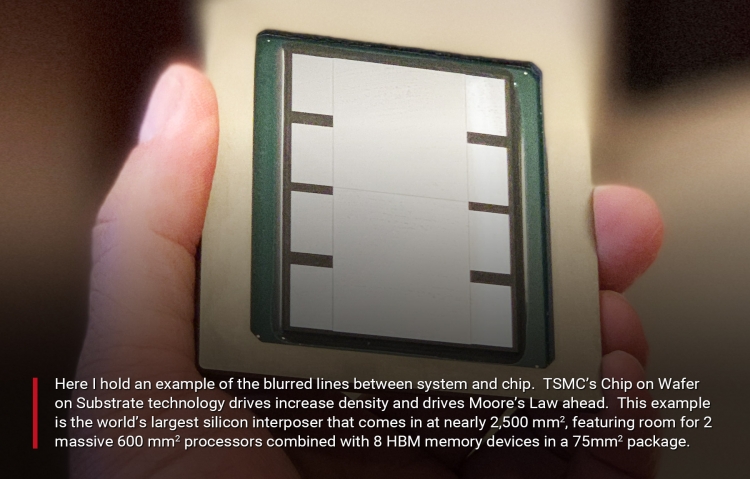
Godfrey did show one big tease - a TSMC’s chip on wafer or substrate technology with a massive 2500 mm2 interposer. The interposer bonds two massive 600 mm2 processors combined with eight HBM memory chips in 75 mm2 packages.
Vega 7 is 331 mm2 while the Tesla V100 is one of the biggest chips ever built with 815 mm² size and 21 billion transistors at 12nm. Bearing that in mind, TSMC has a solution for two 600 mm cores that will be able to accommodate dramatically more transistors in the same area in N5P or even in N5 5nm process.
2500 mm2 interposer and two 600mm2 chips and 8 HBM chips
The 2500 mm2 interposer with so many memory and dual chips would do a lot of AI-related calculations, and we all know that there are a lot of calculations needed for the ADAS and self-driving, medicine, new material research, fuel efficiency and anything that needs optimization including band and stock transactions.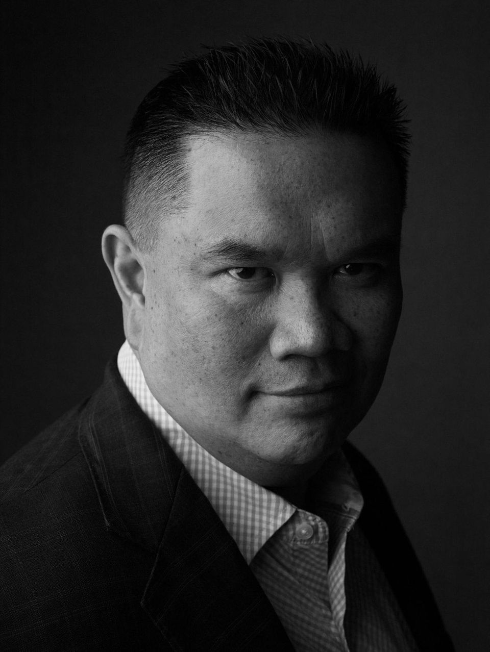
Godfrey who we know from ATI, AMD and most recently as an EVP of the market at Synaptics, has the chance to help TSMC get more much-needed exposure and coverage, as frankly, this is currently the best manufacturing facility especially when it comes to cutting edge technology including 7nm and 5nm. The 5nm process is just around the corner, and as a performance enthusiast, we cannot wait to learn more.