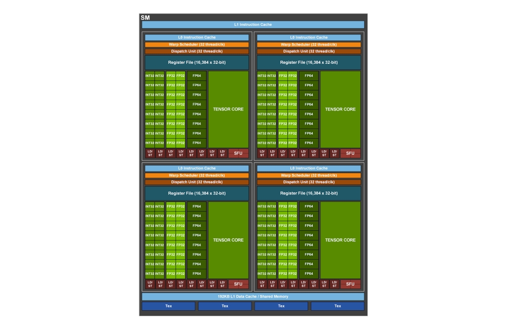
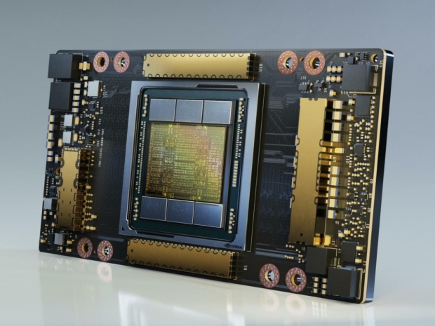
Manufactured on TSMC's 7nm N7 manufacturing process, the GA100 is a compute beast with 54 billion transistors on 826mm2 die size. It packs 8 GPU Processing Clusters (GPCs) with 8 Texture Processing Clusters per GPC, two Streaming Multiprocessors (SMs) per TPC, and 16 SMs per GPC.
All of these numbers translate to a total of 128 SMs for a full GA100 GPU, and with 64 FP32 CUDA cores per SM, this adds up to an impressive total of 8,192 FP32 CUDA cores.
The GA100 also has 6 HBM2 2.4Gbps stacks with 12 512-bit memory controllers (5 HBM2 stacks and 10 512-bit controllers for A100), leaving it with 48GB of VRAM on a 6144-bit memory interface, We did not get the official compute performance numbers for the fully enabled GA100 GPU, but judging from the A100 numbers, the GA100 is an impressive beast.
The GPU also comes with four 3rd generation Tensor Cores per SM, which means 512 Tensor Cores for a full GPU.


The third generation Tensor Core makes a difference
What makes the GA100 such a compute beast are the 3rd generation Tensor Cores, which bring significant improvements, including acceleration for all data types, including FP16, BF16, TF32, FP64, INT8, INT4, and Binary.
It also features 192KB of combined shared memory and L1 data cache, new asynchronous copy instruction loads data directly from global memory into shared memory and can be used with shared-memory-based barrier unit, new instructions for L2 cache management and residency controls, new warp-level reduction instructions, as well as many other programmability improvements to reduce software complexity.
Bear in mind that GA100 packs 512 of 3rd gen Tensor Cores per GPU (432 for the A100), and these add up to some impressive compute performance.
The GA100-based A100 Tensor Core GPU has 7 GPCs for 108 SMs and 6912 FP32 CUDA cores per GPU
We'll first see the GA100 GPU in the A100 Tensor Core GPU, which will be a part of Nvidia's newly announced DGX A100 AI system.
Also read
Nvidia unveils the A100 Tensor Core GPU


