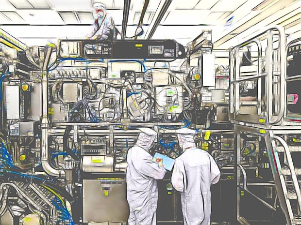
While chips have traditionally been packaged with one silicon tile inside companies are stacking several of them to improve performance. The downside of this is that it makes testing a nightmare as there are variations between layers.
Siemens’ head of the Tessent business Ankur Gupta said until now Siemens has had to work with customers on a case-by-case basis.
“What we are doing now is taking all of those learnings and automating the solution, making it available general purpose for everybody to use,” Gupta told Reuters.
He said making the testing process easier for chips with advanced packaging, also referred to as 2.5 and 3-dimensional packaging, will help give the new technology a boost.


