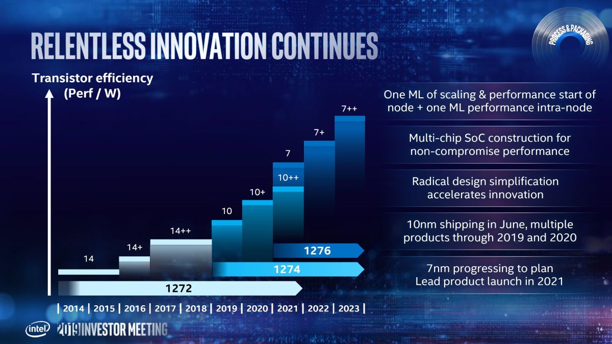
Intel’s Murthy Renduchintala provided first updates on Intel’s 7nm process technology expected to deliver two times scaling. Murthy mentioned that Intel plans to provide approximately 20 percent increase in performance per watt with a four times reduction in design rule complexity.
Intel already announced that it plans to launch a 10nm discrete GPU in 2020 and, the year after it looks like it will transition from 10nm to 7nm, at least for the data center part. This would get Intel back to its original two year cadence to transition to a new manufacturing node. So far, TSMC did a good job moving from 14nm to 10nm to current 2nd generation 7nm, and it is expected that TSMC will have 5nm in 2021.
Intel’s 7nm comparable to TSMC’s 5nm
It is imperative to mentation that Intel is using extreme ultraviolet (EUV) lithography for its 7nm technology and this is what TSMC is using for its 5nm. Samsung's fabrication facilities use EUV for its upcoming 5nm too expected in 2021 timeframe.
Many processor manufacturing experts we talked to have compared Intel’s 10nm with TSMCs 7nm and that this number is more marketing than anything else. It is to expect that Intel’s 7nm will be comparable with TSMC’s 5nm.
Murthy also mentioned that the 7nm mark Intel’s first commercial use of extreme ultraviolet (EUV) lithography, a technology that will help drive scaling for multiple node generations. A process that Intel calls 1276 should be a designation for the 7nm. The 1276 starts in 2021 and already in 2022 Intel mentions 7+, a year after it is a time of 7++.
Intra node optimizations
Murthy has mentioned that Intel learned quite a bit from 14nm and that the company managed to squeeze more than 20 percent transistor efficiency between Broadwell 2014 and Whiskey Lake client processors launched in late 2018. The turbo performance increased by 30 percent.
This revealed another important lesson that Intel is now institutionalizing. Intel now deliberately plans for intra node optimizations. That is how Intel plans to have 10nm, a year later 10+ and a year after that it is time for 10++. Parallel to this roadmap and intra node optimizations, Intel will start 7nm in 2021.
The chiplet mix nodes theory
The chiplet theory is becoming increasingly important as the value in maintaining the mixed nodes will give business units the flexibility to optimize for product performance, time to market and margin. Intel has to make it easy and fast for its development teams to migrate their designs through an intra node design transitions. Murthy explained that 7nm is the first node to completely implement the intra node optimizations and intra nodes design practice. The schedule and time to market are Intel’s priority and greater than 15 percent transistor efficiency is to be expected in gen over gen.
The 7nm transition is also aligned with Intel’s next-generation packaging technologies - the next-gen Foveros and EMIB. The introduction of 7nm will overlap with the last node of 10, called 10++ in 2021.
Xe based GP-GPU in 2021
The lead 7nm product is expected to be an Intel Xe architecture-based, general-purpose GPU for data center AI and high-performance computing. It follows a heterogeneous approach to product construction using advanced packaging technology.
On the heels of Intel’s first discrete GPU coming in 2020, the 7nm general-purpose GPU is expected to launch in 2021. Yes, this sentence is a shot in Nvidia’s direction and an early warning for financial analysts that the big battle in both AI, data and gaming market is coming in years ahead of us.
Intel’s sees a 7nm GP GPU as a major strategic priority for Intel and describes it as a groundbreaking GP GPU product targeted for Intel Datacenter AI and HPC. It will embody a new heterogeneous approach to product construction and use Intel’s advanced packaging capabilities.
The 2021 launch date is aligned with Intel’s design win with the Department of Energy to deliver the US first Exoflop (10 to the 18, quintillion operation) capable computer named Aurora.


