GlobalFoundries should be rolling out 20nm chips later this year and we hope that some AMD 20nm products might actually launch this year. The foundry failed to conquer the world with its 28nm process, but after some delays it got sorted out the problems and managed to ship some high-volume parts based on this process.
GlobalFoundries is manufacturing AMD’s new Kaveri APUs, while TSMC is making the Jaguar-based 28nm parts. We are not sure who is making the new server parts such as Seattle or Berlin, both 28nm designs. It is expected that GlobalFoundries should commence volume production of some 20nm parts later this year and the company has big plans for a faster transition to 14nm.
GlobalFoundries cozying up to Samsung
It is no secret that Intel leads the way in new process transitions and that Intel plans to ship 14nm parts at the time TSMC and GlobalFoundries are struggling to ship their first 20nm parts.

GlobalFoundries has now announced that it will start a strategic collaboration with none other than Samsung for its 14nm transition. It is easy to see that these two big players need each other in order to fight against bigger competitors like Intel and TSMC. GlobalFoundries and Samsung don’t have much overlap, either.
This joint venture will result in faster time-to-market for 14nm FinFET-based products. We see at least two advantages. According to Ana Hunter, Vice President of Product Management at GlobalFoundries, the process design kits are available today and the the foundry should be ready to manufacture 14nm FinFET products by the end of 2014. This sounds a bit optimistic, as we heard these bold announcements before, especially as both companies didn’t really start shipping 20nm parts yet, at least not in high volume high performance parts. It should be noted that Samsung joined the 28nm club quite late and shipped its first 28nm SoC just a year ago, in the Galaxy S4.

Sawn Han, Vice president of foundry marketing at Samsung Electronics, calls this partnership a ‘game changer’ as it will enable 14nm production by a total of four foundries in the world, three from Samsung and one from GlobalFoundries. Samsung will offer 14nm FinFET from S2 Fab in Austin Texas, S3 Fab in Hwa Seong in South Korea and S1 Fab in Gi Heung South Korea. GlobalFoundries is preparing its Fab 8 in Saratoga, New York State, for the 14nm push.
14nm FinFET crucial for next-gen SoC designs
The companies say 14nm FinFET technology features a smaller contact gate pitch for higher logic packing density and smaller SRAM bitcells to meet the increasing demand for memory content in advanced SoCs, while still leveraging the proven interconnect scheme from 20nm to offer the benefits of FinFET technology with reduced risk and the fastest time-to-market.

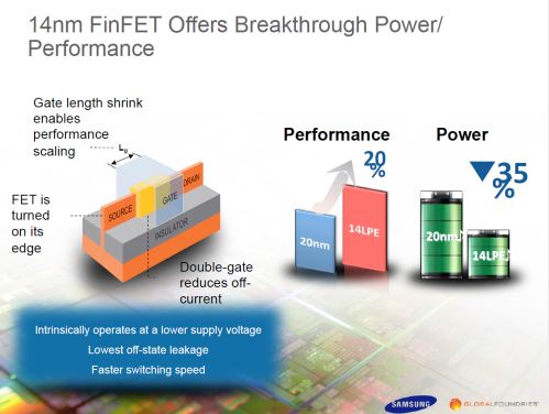
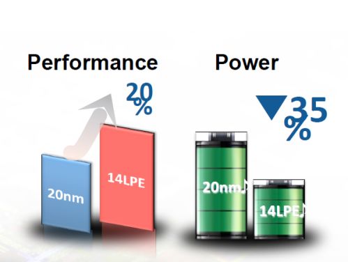
The 14nm LPE should deliver 20 percent more performance compared to 20nm parts and the power required should sink 35 percent versus 20nm LPE parts. Compared to 20nm parts it will save 15 percent of die space as well making it possible to cram more components into the same die size.
We have yet to see the first mobile 20nm parts in actual products. Qualcomm announced its first Snapdragons based on the new process a few weeks ago, but they won’t be ready for months. You can expect that a SoC manufactured on 14nm could end up 40 to 50 percent faster than its 28nm predecessor and that the power requirement could go down by 50 to 70 percent at best.
The total market for mobility, wireless and computer network storage market is expected to hit around $20 billion by 2017. Of course, everyone wants the piece of that action. The joint venture will offer both 14nm LPE (Low Power Enhanced) and 14nm LPP (Laser-Produced Plasma) process.
All we need now are the design wins from high-volume customers and if we were to bet we would place our money on Samsung, namely its Exynos processors. We would be positively surprised to see 14nm SoC in mobile phones and tablets in 2015, but it is a possibility. Keep in mind that we are still waiting to see the first 20nm SoCs and GPUs in action.


